錚?/div>
Low On-State Resistance
Avalanche and Surge Rated
High Frequency Switching
Ultra Low Leakage current
UIS rated
Available with Lot Acceptance Testing
SURFACE MOUNT
N 鈥?CHANNEL
MOSFET
Description
This device is an N-Channel enhancement mode, high density MOSFET.
It is passivated with 4 um (40 kA) of oxynitride, and supplied in a three
leaded package.
Maximum Ratings
PARAMETER
SYMBOL
VALUE
1000
Drain-to-Source Voltage
V
DSS
V
GS
+/- 20
Gate- to -Source Voltage
Continuous Drain Current @ TC = 25擄C
I
D1
1.0
擄
Continuous Drain Current @ TC=100擄C
I
D2
0.27
擄
1.0
Avalanche Current
I
AR
3.5
Repetitive Avalanche Energy
E
AR
120
Single Pulse Avalanche Energy
E
AS
Operating & Storage Junction Temperature Range T
J
, T
STG
- 40 to +125
Steady-state Thermal Resistance, Junction-to-Tab R胃
J-TAB
2.5
胃
UNIT
Volts
Volts
Amps
Amps
Amps
mJ
mJ
擄
C
擄
C/Watt
Static Electrical Characteristics
SYMBOL
BV
DSS
V
GS(TH)2
V
GS(TH)1
R
DS(ON)1
R
DS(ON)2
R
DS(ON)3
R
DS(ON)4
R
DS(ON)5
I
DSS1
I
DSS2
I
GSS1
I
GSS2
I
GSS3
CHARACTERISTICS / TEST CONDITIONS
Drain to Source Breakdown Voltage
(VGS=0V, ID=0.25mA)
Gate Threshold Voltage
(VGS=VDS, ID=1mA, TJ=37擄C )
擄
Gate Threshold Voltage
(VGS=VDS, ID=1mA, TJ=25擄C )
擄
Drain to Source ON-State Resistance
(VGS=10V, ID=ID 1 , TJ=25擄C )
擄
Drain to Source ON-State Resistance (VGS=7V, ID=5鈥?50ma, TJ=37擄C)
擄
Drain to Source ON-State Resistance (VGS=7V, ID=5鈥?50ma, TJ=25擄C)
擄
Drain to Source ON-State Resistance (VGS=7V, ID=5鈥?50ma, TJ=60擄C)
擄
Drain to Source ON-State Resistance
(VGS=7V, ID=ID 1 , TJ=125擄C )
擄
Zero Gate Voltage-Drain Current (VDS=80%BVDSS,VGS=0V,TJ= 25擄C )
擄
Zero Gate Voltage-Drain Current (VDS=80%BVDSS,VGS=0V,TJ=125擄C )
擄
Gate to Source Leakage Current
(VGS=
鹵
20V, VDS=0V, TJ = 25擄C )
擄
Gate to Source Leakage Current
(VGS=
鹵
20V, VDS=0V, TJ = 37擄C )
擄
Gate to Source Leakage Current
(VGS=
鹵
20V, VDS=0V, TJ=125擄C )
擄
MIN
1000
2
TYP
3.4
3.5
12.5
12.5
11.5
15.0
25.5
MAX
UNIT
Volts
Volts
Volts
Ohms
Ohms
Ohms
Ohms
Ohms
uA
uA
nA
nA
uA
4.5
13.5
25
250
鹵
100
10.0
25
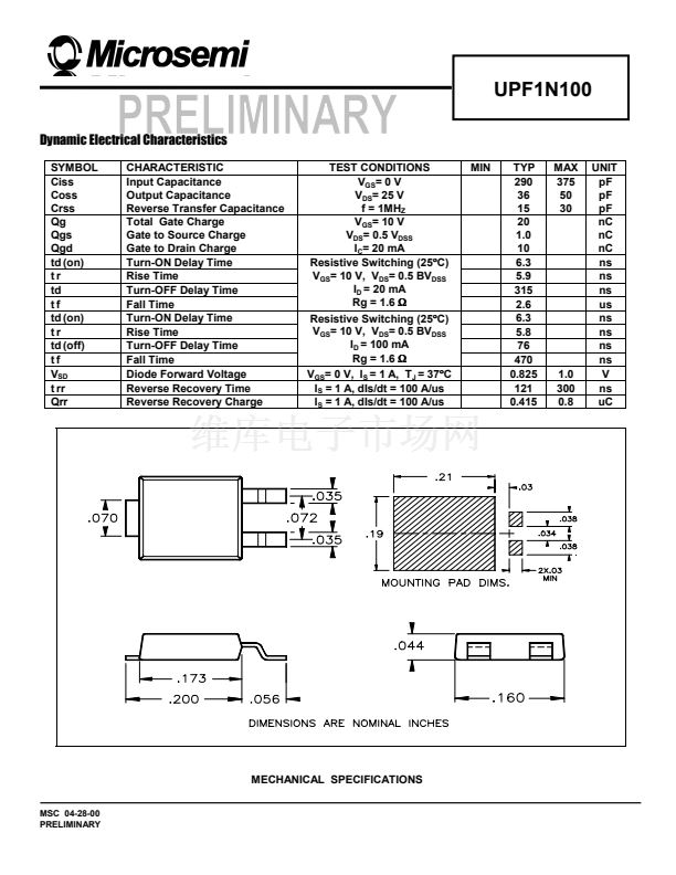
MSC 04-28-00
PRELIMINARY


 1
1
 2
2
