鈥?/div>
OPERATING FREQUENCY:
50 to 150 MHz
I/Q INPUT FREQUENCY RANGE:
DC to 500 kHz
DIGITAL 90
擄
PHASE SHIFTER
ALLOWABLE BIAS VOLTAGE:
2.7 to 5.5 V
POWER SAVE: "SLEEP" MODE
SMALL SIZE SSOP20 SURFACE MOUNT PACKAGE
TAPE AND REEL PACKAGING OPTION AVAILABLE
UPC8101GR
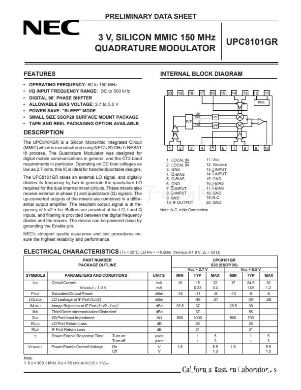
INTERNAL BLOCK DIAGRAM
13
20
19
18
17
16
15
14
12
11
REG.
F/F
90藲
270藲
0藲
180藲
LPF
LPF
DESCRIPTION
The UPC8101GR is a Silicon Monolithic Integrated Circuit
(MMIC) which is manufactured using NEC's 20 GHz f
T
NESAT
III process. The Quadrature Modulator was designed for
digital mobile communications in general, and the CT2 band
requirements in particular. Operating on DC bias voltages as
low as 2.7 volts, this IC is ideal for handheld/portable designs.
The UPC8101GR takes an external LO signal, and digitally
divides its frequency by two to generate the quadrature LO
required for the dual internal mixer circuits. These mixers also
receive external in-phase (I) and quadrature (Q) signals. The
up-converted outputs of the mixers are combined in a differ-
ential output amplifier. The resultant output signal is at fre-
quency of f
LO
/2 + f
I/Q
. Buffers are provided at the LO, I and Q
inputs, and filtering is provided between the digital frequency
divider and the mixers. The device can be powered down by
grounding the Enable pin.
NEC's stringent quality assurance and test procedures en-
sure the highest reliability and performance.
1
2
3
4
5
6
7
8
9
10
1. LOCAL IN
2. LOCAL IN
3. GND
4. Q-BIAS
5. Q-BIAS
6. GND
7. Q-INPUT
8. Q-INPUT
9. GND
10. IF OUTPUT
11. V
CC
12. V
ENABLE
13. I-INPUT
14. I-INPUT
15. GND
16. I-BIAS
17. I-BIAS
18. GND
19. N.C.
20. GND
Note: N.C. = No Connection
ELECTRICAL CHARACTERISTICS
(T
A
= 25擄C, LO P
IN
= -10 dBm, V
ENABLE
鈯?.8
V, Z
L
= 50
鈩?
PART NUMBER
PACKAGE OUTLINE
V
CC
= 2.7 V
SYMBOLS
I
CC
P
SAT
LO
LEAK
IM
REJ
IM
3
Z
I/Q
RL
LO
RL
IF
PARAMETERS AND CONDITIONS
Circuit Current
V
ENABLE
鈮?/div>
1.0 V
Saturated Output Power
LO Leakage at IF Port (f
LO
/2)
Image Rejection at IF Port (f
LO
/2 -
I/Q Port Input Impedance
LO Port Return Loss
IF Port Return Loss
Power Enable Response Time
Power Enable Control Voltage
Turn on
Turn off
On
Off
f
I/Q
)
1
Third Order Intermodulation Distortion
1
UNITS
mA
mA
dBm
dBm
dBc
dBc
K鈩?/div>
dB
dB
碌sec
碌sec
V
V
1.8
500
28.5
MIN
10
-16
TYP
15
0.33
-11
-49
37
37
1000
26
21
1
1
5
3
5.5
1.0
1.8
500
MAX
22
0.4
-8
-37
28.5
MIN
17
-13
UPC8101GR
S20 (SSOP 20)
V
CC
= 5.5 V
TYP
24.5
1.05
-8
-39
38
56
700
26
21
1
1
5
3
5.5
1.0
MAX
32
1.2
-5
-28
蟿
V
ENABLE
Note:
1. f
LO
= 300.1 MHz, f
I/Q
= 36 kHz at V
CC
/2 + 1 V
p-p
.
California Eastern Laboratories


 1
1
 2
2
 3
3
