鈥?/div>
5
4
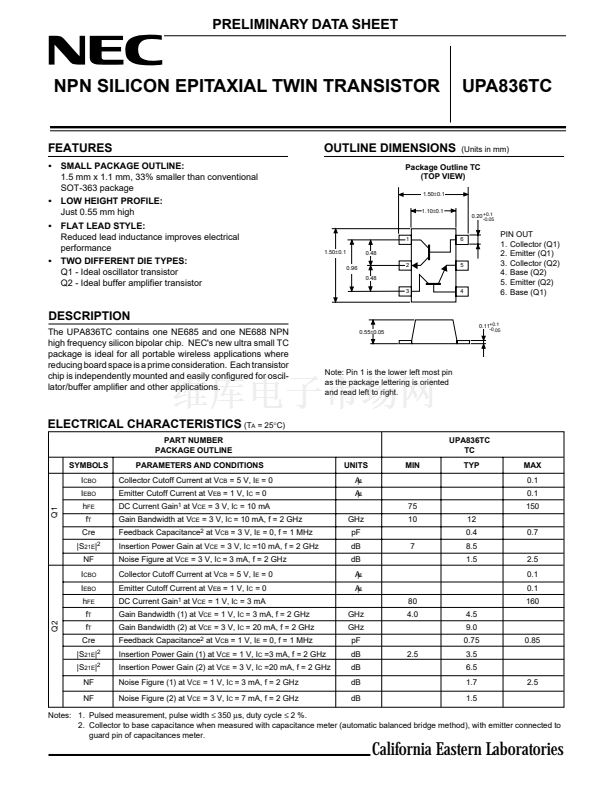
PIN OUT
1. Collector (Q1)
2. Emitter (Q1)
3. Collector (Q2)
4. Base (Q2)
5. Emitter (Q2)
6. Base (Q1)
DESCRIPTION
The UPA836TC contains one NE685 and one NE688 NPN
high frequency silicon bipolar chip. NEC's new ultra small TC
package is ideal for all portable wireless applications where
reducing board space is a prime consideration. Each transistor
chip is independently mounted and easily configured for oscil-
lator/buffer amplifier and other applications.
0.11
+0.1
0.55鹵0.05
-0.05
Note: Pin 1 is the lower left most pin
as the package lettering is oriented
and read left to right.
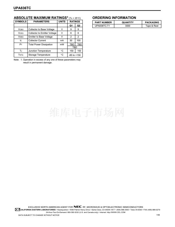
ELECTRICAL CHARACTERISTICS
(T
A
= 25擄C)
PART NUMBER
PACKAGE OUTLINE
SYMBOLS
I
CBO
I
EBO
h
FE
f
T
Cre
|S
21E
|
2
NF
I
CBO
I
EBO
h
FE
f
T
PARAMETERS AND CONDITIONS
Collector Cutoff Current at V
CB
= 5 V, I
E
= 0
Emitter Cutoff Current at V
EB
= 1 V, I
C
= 0
DC Current Gain
1
at V
CE
= 3 V, I
C
= 10 mA
Gain Bandwidth at V
CE
= 3 V, I
C
= 10 mA, f = 2 GHz
Feedback
Capacitance
2
at V
CB
= 3 V, I
E
= 0, f = 1 MHz
Insertion Power Gain at V
CE
= 3 V, I
C
=10 mA, f = 2 GHz
Noise Figure at V
CE
= 3 V, I
C
= 3 mA, f = 2 GHz
Collector Cutoff Current at V
CB
= 5 V, I
E
= 0
Emitter Cutoff Current at V
EB
= 1 V, I
C
= 0
DC Current
Gain
1
at
V
CE
= 1 V, I
C
= 3 mA
GHz
GHz
pF
dB
dB
dB
dB
2.5
Gain Bandwidth (1) at V
CE
= 1 V, I
C
= 3 mA, f = 2 GHz
Gain Bandwidth (2) at V
CE
= 3 V, I
C
= 20 mA, f = 2 GHz
Feedback Capacitance
2
at V
CB
= 1 V, I
E
= 0, f = 1 MHz
Insertion Power Gain (1) at V
CE
= 1 V, I
C
=3 mA, f = 2 GHz
Insertion Power Gain (2) at V
CE
= 3 V, I
C
=20 mA, f = 2 GHz
Noise Figure (1) at V
CE
= 1 V, I
C
= 3 mA, f = 2 GHz
Noise Figure (2) at V
CE
= 3 V, I
C
= 7 mA, f = 2 GHz
GHz
pF
dB
dB
碌A(chǔ)
碌A(chǔ)
80
4.0
4.5
9.0
0.75
3.5
6.5
1.7
1.5
2.5
0.85
7
UNITS
碌A(chǔ)
碌A(chǔ)
75
10
12
0.4
8.5
1.5
2.5
0.1
0.1
160
0.7
MIN
UPA836TC
TC
TYP
MAX
0.1
0.1
150
Q2
Q1
f
T
Cre
|S
21E
|
2
|S
21E
|
2
NF
NF
Notes: 1. Pulsed measurement, pulse width
鈮?/div>
350
碌s,
duty cycle
鈮?/div>
2 %.
2. Collector to base capacitance when measured with capacitance meter (automatic balanced bridge method), with emitter connected to
guard pin of capacitances meter.
California Eastern Laboratories


 1
1
 2
2
