DATA SHEET
MOS FIELD EFFECT POWER TRANSISTORS
碌
PA1753
SWITCHING
DUAL N-CHANNEL POWER MOS FET
INDUSTRIAL USE
DESCRIPTION
This product is Dual N-Channel MOS Field Ef-
fect Transistor designed for power management
application of notebook computers, and Li-ion bat-
tery application.
8
PACKAGE DIMENSIONS
(in: millimeter)
5
1 ; Source 1
2 ; Gate 1
7, 8 ; Drain 1
3 ; Source 2
4 ; Gate 2
5, 6 ; Drain 2
1
1.44
FEATURES
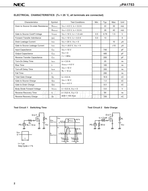
鈥?Dual MOSFET chips in small package
鈥?2.5 V Gate Drive Type and Low On-Resistance
R
DS(on)1
= 30 m鈩?Max. (V
GS
= 4.5 V, I
D
= 3.0 A)
R
DS(on)2
= 40 m鈩?Max. (V
GS
= 2.5 V, I
D
= 3.0 A)
1.8 Max.
4
5.37 Max.
+0.10
鈥?.05
6.0 鹵0.3
4.4
0.8
鈥?Low C
iss
C
iss
= 740 pF Typ.
鈥?Built-in G-S Protection Diode
鈥?Small and Surface Mount Package
(Power SOP8)
0.15
0.05 Min.
0.5 鹵0.2
0.10
1.27
0.40
0.78 Max.
0.12 M
+0.10
鈥?.05
ABSOLUTE MAXIMUM RATINGS (T
A
= 25 藲C, all terminals are connected)
Drain to Source Voltage
Gate to Source Voltage
Drain Current (DC)
Drain Current (pulse)
Note 1
Total Power Dissipation (1 unit)
Note 2
Total Power Dissipation (2 unit)
Note 2
Channel Temperature
Storage Temperature
V
DSS
V
GSS
I
D(DC)
I
D(pulse)
P
T
P
T
T
ch
T
stg
20
鹵8.0
鹵6.0
鹵24
1.7
2.0
150
鈥?5 to +150
V
V
A
A
W
W
藲C
藲C
Gate
Protection
Diode
Gate
Drain
Body
Diode
Source
Notes 1.
PW
鈮?/div>
10
碌
s, Duty Cycle
鈮?/div>
1 %
2.
T
A
= 25 藲C, Mounted on ceramic substrate of 2000 mm
2
脳
1.1 mm
The diode connected between the gate and source of the transistor serves as a protector against ESD. When this
device acutally used, an additional protection circuit is externally required if voltage exceeding the rated voltage may
be applied to this device.
The information in this document is subject to change without notice.
Document No. D11496EJ2V0DS00 (2nd edition)
Date Published October 1996 N
Printed in Japan
漏
1996


 1
1
 2
2
 3
3
 4
4
 5
5
 6
6
 7
7
 8
8
