鈩?/div>
Conditions
I
D
=
10
碌A,
V
GS
=
0
V
DS
=
50 V, V
GS
=
0
V
GS
= 鹵7
V, V
DS
=
0
I
D
=
1
碌A,
V
DS
=
3 V
I
D
=
10 mA, V
GS
=
2.5 V
I
D
=
10 mA, V
GS
=
4.0 V
Forward transfer admittance
Input capacitance
Output capacitance
Reverse transfer capacitance
Turn-on time
*
Turn-off time
*
I
D
=
10 mA, V
DS
=
4.0 V
V
DS
=
3 V, V
GS
=
0 V, f
=
1 MHz
20
0.9
1.2
8
6
60
12
7
3
200
200
Min
50
1.0
鹵5
1.5
15
12
mS
pF
pF
pF
ns
ns
Typ
Max
Unit
V
碌A
碌A
V
鈩?/div>
Note) *: Refer to t
on
, t
off
test circuit (next page)
0.10 max
Publication date: July 2002
SJJ00265AED
1


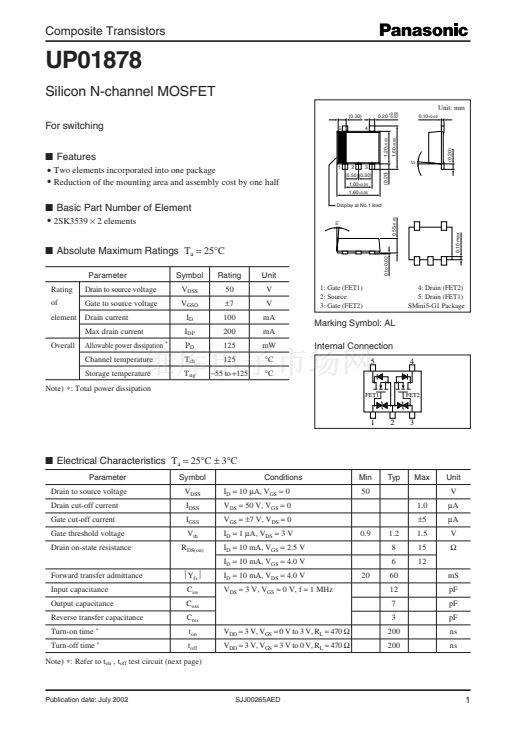 1
1
 2
2
 3
3
