UCC2918/81510
LOW ON RESISTANCE HOT SWAP POWER MANAGER
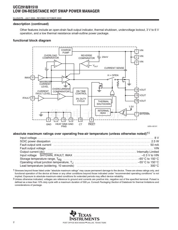
SLUS457B 鈥?JULY 2000 - REVISED OCTOBER 2000
D
Integrated 0.075-鈩?Power MOSFET
D
3 V to 6 V Operation
D
External Analog Control of Fault Current
D
D
D
D
D
D
D
D
From 0 A to 4 A
Independent Analog Control of Current
Limit up to 5 A
Fast Overload Protection
Unidirectional Switch
Minimal External Components
1-碌A(chǔ) I
CC
When Disabled
Programmable On Time
Programmable Start Delay
Fixed 3% Duty Cycle
N and DP PACKAGES
(TOP VIEW)
VIN
VIN
VIN
GND*
GND*
FAULT
SHTDWN
IFAULT
1
2
3
4
5
6
7
8
16
15
14
13
12
11
10
9
VOUT
VOUT
VOUT
GND*
GND*
NC
CT
IMAX
Pin 5 serves as the lowest impedance to the electrical
ground. Pins 4, 12, and 13, serve as heat sink/ground.
These pins should be connected to large etch PCB areas
to help dissipate heat. For N package, pins 4, 12, and 13,
are NC.
description
The UCC2918 low on-resistance hot swap power
manager provides complete power management, hot
swap capability, and circuit breaker functions. The only
VIN
components needed to operate the device, other than
VIN
supply bypassing, are a timing capacitor and two
VIN
programming resistors. All control and housekeeping
VIN
functions are integrated and externally programmable.
GND*
These include the fault current level, maximum output
GND*
sourcing current, maximum fault time, and startup
GND*
delay. In the event of a constant fault, the internal fixed
GND*
3% duty cycle ratio limits the average output power. The
GND*
IFAULT pin allows linear programming of the fault level
FAULT
current from 0 A to 4 A.
SHTDWN
Fast overload protection is accomplished by an
additional overload comparator. Its threshold is
internally set above the maximum sourcing current limit
setting. In the event of a short circuit or extreme current
condition, this comparator is tripped, shutting down the
output. This function is needed since the maximum
sourcing current limit loop has a finite bandwidth.
IFAULT
PWP PACKAGE
(TOP VIEW)
1
2
3
4
5
6
7
8
9
10
11
12
24
23
22
21
20
19
18
17
16
15
14
13
VOUT
VOUT
VOUT
VOUT
GND*
GND*
GND*
GND*
GND*
NC
CT
IMAX
Pin 9 serves as the lowest impedance to the electrical
ground. Pins 5, 6, 7, 8, 16, 17, 18, 19, and 20 serve as
heat sink/ground.
When the output current is below the fault level, the output MOSFET is switched on with a nominal resistance
of 0.075
鈩?
When the output current exceeds the fault level or the maximum sourcing level, the output remains
on, but the fault timer starts charging a capacitor connected to the CT pin (C
T
). Once C
T
charges to a preset
threshold, the switch is turned off, and remains off for 30 times the programmed fault time. When the output
current reaches the maximum sourcing level, the MOSFET transitions from a switch to a constant current
source.
The UCC2918 is designed for unidirectional current flow, emulating an ideal diode in series with the power
switch. This feature is particularly attractive in applications where many devices are powering a common bus,
such as with SCSI termintation power (Termpwr). The UCC2918 can also be put into the sleep mode, drawing
only 1
碌A(chǔ)
of supply current.
Please be aware that an important notice concerning availability, standard warranty, and use in critical applications of
Texas Instruments semiconductor products and disclaimers thereto appears at the end of this data sheet.
PRODUCTION DATA information is current as of publication date.
Products conform to specifications per the terms of Texas Instruments
standard warranty. Production processing does not necessarily include
testing of all parameters.
Copyright
漏
2000, Texas Instruments Incorporated
POST OFFICE BOX 655303
鈥?/div>
DALLAS, TEXAS 75265
1


 1
1
 2
2
 3
3
 4
4
 5
5
 6
6
 7
7
 8
8
 9
9
 10
10
