鈥?/div>
3pF Channel Capacitance
DESCRIPTION
The UCC5630 Multi-Mode Low Voltage Differential and Single Ended Ter-
minator is both a single ended terminator and a low voltage differential ter-
minator for the transition to the next generation SCSI Parallel Interface
(SPI-2). The low voltage differential is a requirement for the higher speeds
at a reasonable cost and is the only way to have adequate skew budgets.
The transceivers can be incorporated into the controller, unlike SCSI high
power differential (EIA485) which requires external transceivers. Low Volt-
age differential is specified for Fast-40 and Fast-80, but has the potential of
speeds up to Fast-320. The UCC5630 is SPI-2, SPI and Fast-20 compliant.
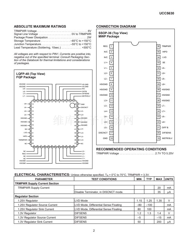
Consult SSOP-36 and LQFP-48 Package Diagram for exact dimensions.
The UCC5630 can not be used with SCSI high voltage differential (HVD)
EIA485. It will shut down when it sees high power differential to protect the
bus. The pinning for high power differential is not the same as LVD or sin-
gle ended and the bias voltage, current and power are also different for
EIA485 differential.
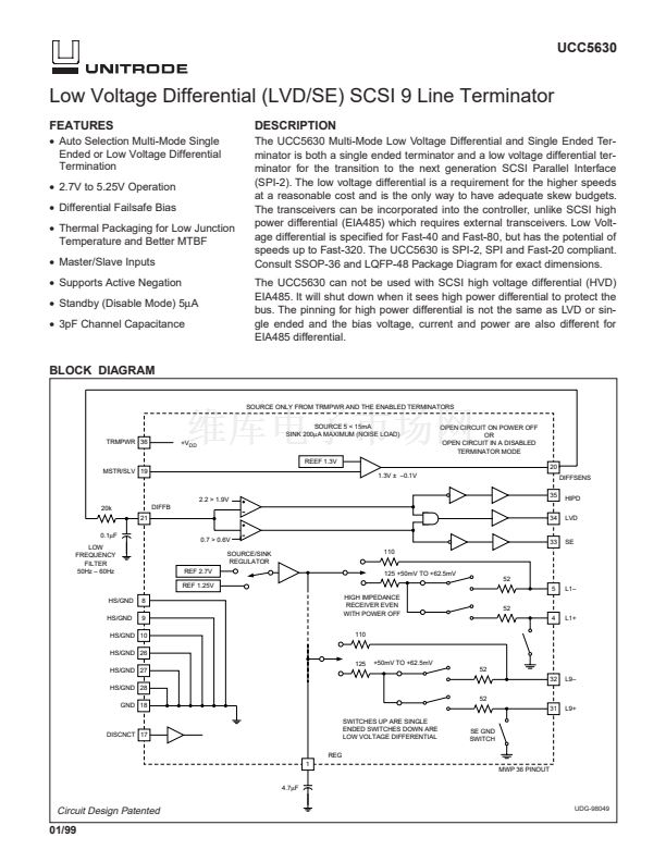
BLOCK DIAGRAM
SOURCE ONLY FROM TRMPWR AND THE ENABLED TERMINATORS
SOURCE 5 < 15mA
SINK 200碌A(chǔ) MAXIMUM (NOISE LOAD)
TRMPWR 36
+V
DD
REEF 1.3V
MSTR/SLV 19
1.3V 鹵 鈥?.1V
35
OPEN CIRCUIT ON POWER OFF
OR
OPEN CIRCUIT IN A DISABLED
TERMINATOR MODE
20
DIFFSENS
HIPD
LVD
2.2 > 1.9V
20k
21
0.1碌F
LOW
FREQUENCY
FILTER
50Hz 鈥?60Hz
0.7 > 0.6V
SOURCE/SINK
REGULATOR
REF 2.7V
REF 1.25V
HS/GND
HS/GND
8
9
HIGH IMPEDANCE
RECEIVER EVEN
WITH POWER OFF
110
110
125 +50mV TO +62.5mV
DIFFB
34
33
SE
52
5
52
4
L1+
L1鈥?/div>
HS/GND 10
HS/GND 26
125
HS/GND 27
HS/GND 28
+50mV TO +62.5mV
52
32
52
L9鈥?/div>
GND 18
SWITCHES UP ARE SINGLE
ENDED SWITCHES DOWN ARE
LOW VOLTAGE DIFFERENTIAL
REG
1
MWP 36 PINOUT
31
L9+
DISCNCT 17
SE GND
SWITCH
4.7碌F
Circuit Design Patented
UDG-98049
01/99


 1
1
 2
2
 3
3
 4
4
 5
5
