UCC2941-3, UCC2941-5, UCC2941-ADJ, UCC3941-3, UCC3941-5, UCC3941-ADJ
1 V SYNCHRONOUS BOOST CONVERTER
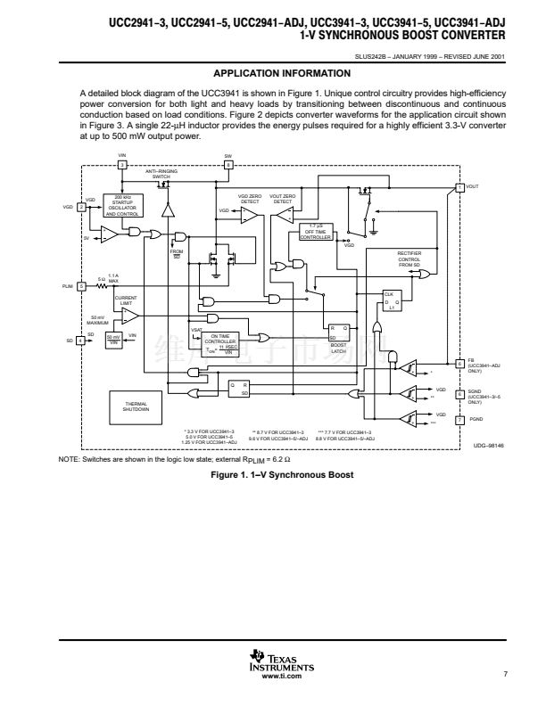
SLUS242B 鈥?JANUARY 1999 鈥?REVISED JUNE 2001
D
1-V Input Voltage Operation Start-up
D
D
D
D
D
D
D
Ensured Under Full Load on Main Output
With Operation Down to 0.4 V
Input Voltage Range of 1 V to V
OUT
+ 0.5 V
500-mW Output Power at Battery Voltages
as Low as 0.8 V
Secondary 9-V Supply From a Single
Inductor
Adjustable Output Power Limit Control
Output Fully Disconnected in Shutdown
Adaptive Current-Mode Control for
Optimum Efficiency
8-碌A(chǔ) Shutdown Supply Current
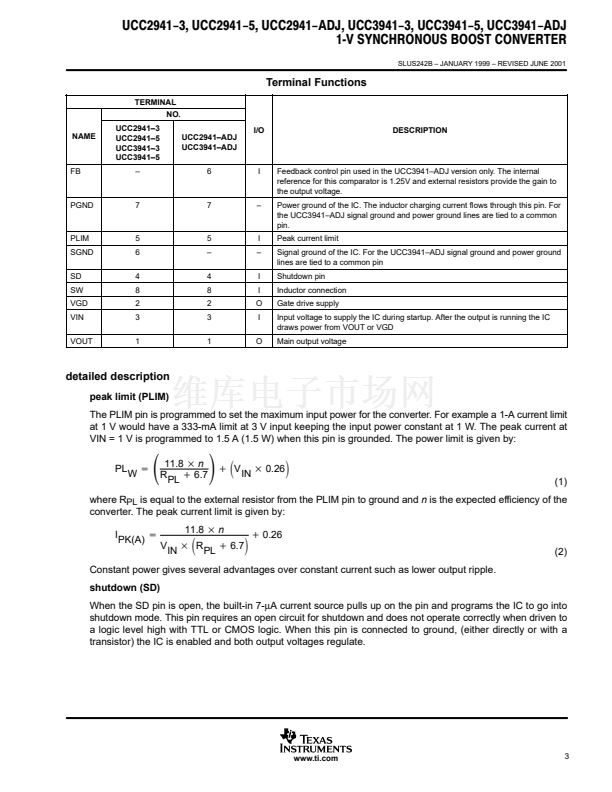
VOUT
VGD
VIN
SD
D OR N PACKAGE
(TOP VIEW)
1
2
3
4
8
7
6
5
SW
PGND
SGND
PLIM
UCC3941鈥揂DJ ONLY
(TOP VIEW)
VOUT
VGD
VIN
SD
1
2
3
4
8
7
6
5
SW
PGND
FB
PLIM
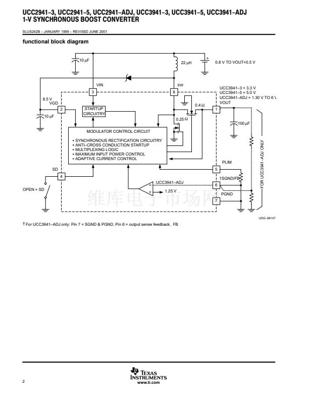
description
The UCC3941 family of low-input-voltage single-inductor boost-converters are optimized to operate from a
single- or dual-alkaline cell, and step up to a 3.3-V, 5-V, or an adjustable output at 500 mW. The UCC3941 family
also provides an auxiliary 9-V, 100-mW output, primarily for the gate drive supply, which can be used for
applications requiring an auxiliary output such as a 5-V supply by linear regulating. The primary output starts
up under full load at input voltages typically as low as 0.8 V, with a guaranteed maximum of 1 V, and operates
down to 0.4 V once the converter is operating, maximizing battery utilization.
Demanding applications such as pagers and personal digital assistants require high efficiency from several
milliwatts to several hundred milliwatts, and the UCC3941 family accommodates these applications with > 80%
typical efficiencies over the wide range of operation. The high-efficiency at low-output current is achieved by
optimizing switching and conduction losses along with low-quiescent current. At higher output current the
0.25-鈩?charge switch, and the 0.4-鈩?synchronous rectifier, along with continuous-mode conduction, provide
high efficiency. The wide input-voltage range on the UCC3941 family can accommodate other power sources
such as NiCd and NiMH.
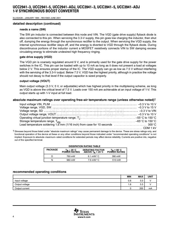
Other features include maximum power control and shutdown control. The device is available in 8-pin SOIC (D)
and 8-pin DIP (N).
AVAILABLE OPTIONS
PACKAGED DEVICES
SOIC (D)
鈥?/div>
TA
3.3
鈥?0_C to 85_C
UCC2941D鈥?
5.0
UCC2941D鈥?
VOUT (V)
Adjustable
3.3
(1.3 V to 6 V)
UCC2941D鈥揂DJ
UCC2941N鈥?
DIP (N)
Adjustable
(1.3 V to 6 V)
UCC2941N鈥揂DJ
5.0
UCC2941N鈥?
0_C to 70_C
UCC3941D鈥? UCC3941D鈥? UCC3941D鈥揂DJ UCC3941N鈥? UCC3941N鈥? UCC3941N鈥揂DJ
鈥?The SOIC (D) package is available left end taped and reeled. Add an R suffix to the device type (e.g., UCC2941DR鈥?) to order
quantities of 2500 devices per reel.
Please be aware that an important notice concerning availability, standard warranty, and use in critical applications of
Texas Instruments semiconductor products and disclaimers thereto appears at the end of this data sheet.
PRODUCTION DATA information is current as of publication date.
Products conform to specifications per the terms of Texas Instruments
standard warranty. Production processing does not necessarily include
testing of all parameters.
Copyright
錚?/div>
2001, Texas Instruments Incorporated
www.ti.com
1


 1
1
 2
2
 3
3
 4
4
 5
5
 6
6
 7
7
 8
8
 9
9
 10
10
 11
11
 12
12
 13
13
 14
14
 15
15
 16
16
 17
17
 18
18
