, Vgs @ - 1.8V, Ids @ - 4.0A = 90m鈩?/div>
D
S
D
S
S
D
G
G
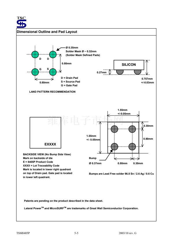
Patent Pending
Description
Bump Side View
TSM8405P is new low cost, state of the art MicroSURF
TM
lateral MOSFET process technology in chip scale bondwireless
packaging minimizes PCB space and Rds(on) plus provides an ultra low Qg x Rds(on) figure of merit.
Features
Low profile package: less than 0.8mm height when
mounted on PCB
Occupies only 2.25mm of PCB area
2
Less than 25% of the area of a SSOT-6
Excellent thermal and electrical capabilities
Lead free solder bumps available
Block Diagram
Ordering Information
Part No.
TSM8405P
Packing
Tape & Reel
Q鈥檛y
3kpcs / 7鈥?/div>
Absolute Maximum Rating
(Ta = 25
o
C
unless otherwise noted)
Parameter
Drain-Source Voltage
Gate-Source Voltage
Continuous Drain Current
Pulsed Drain Current
Maximum Power Dissipation (Steady State)
Operating Junction Temperature
Operating Junction and Storage Temperature Range
Symbol
V
DS
V
GS
I
D
I
DM
P
D
T
J
T
J
, T
STG
Limit
- 12V
鹵8
- 4.9
- 10
1. 5
+150
- 55 to +150
Unit
V
V
A
A
W
o
o
C
C
Thermal Performance
Parameter
Junction to Ambient Thermal Resistance
Junction to Balls Thermal Resistance
Symbol
R
胃ja
R
胃j
R
Limit
85
12
Unit
o
o
C/W
C/W
TSM8405P
1-1
2003/10 rev. G


 1
1
 2
2
 3
3
 4
4
 5
5
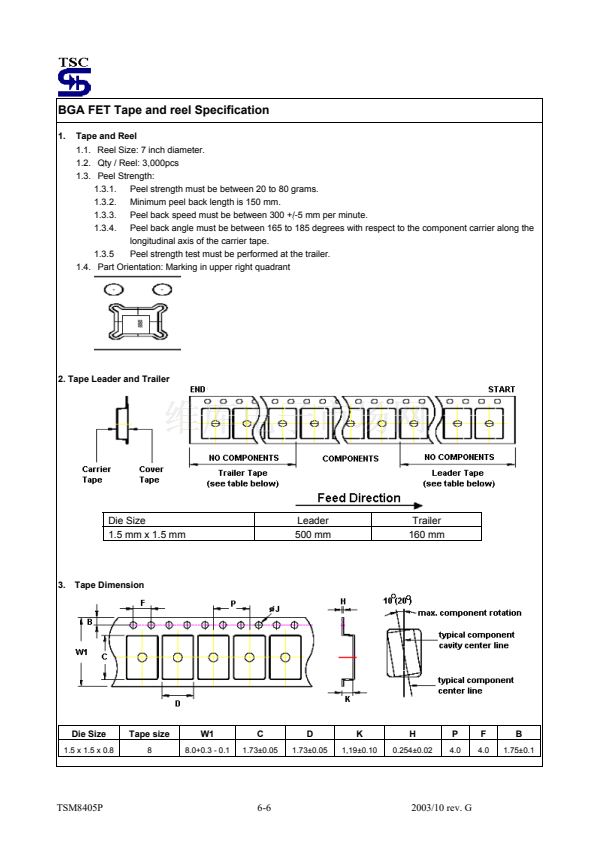 6
6
