, Vgs @ - 2.5V, Ids @ - 2.0A =190m鈩?/div>
Features
Advanced trench process technology
High density cell design for ultra low on-resistance
Excellent thermal and electrical capabilities
Surface mount
Fast switching
Block Diagram
Ordering Information
Part No.
TSM7104DCS
Packing
Tape & Reel
Package
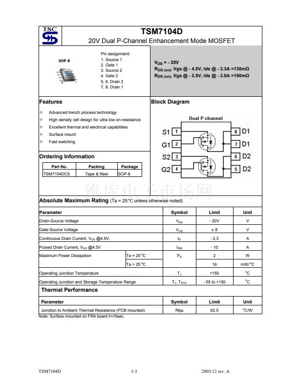
SOP-8
Absolute Maximum Rating
(Ta = 25
o
C
unless otherwise noted)
Parameter
Drain-Source Voltage
Gate-Source Voltage
Continuous Drain Current, V
GS
@4.5V.
Pulsed Drain Current, V
GS
@4.5V
Maximum Power Dissipation
Ta = 25
o
C
Ta > 25 C
Operating Junction Temperature
Operating Junction and Storage Temperature Range
T
J
T
J
, T
STG
o
Symbol
V
DS
V
GS
I
D
I
DM
P
D
Limit
- 20V
鹵8
- 2.3
- 10
2
16
+150
- 55 to +150
Unit
V
V
A
A
W
mW/ C
o
o
o
C
C
Thermal Performance
Parameter
Junction to Ambient Thermal Resistance (PCB mounted)
Note: Surface mounted on FR4 board t<=5sec.
Symbol
R
胃ja
Limit
62.5
Unit
o
C/W
TSM7104D
1-3
2003/12 rev. A


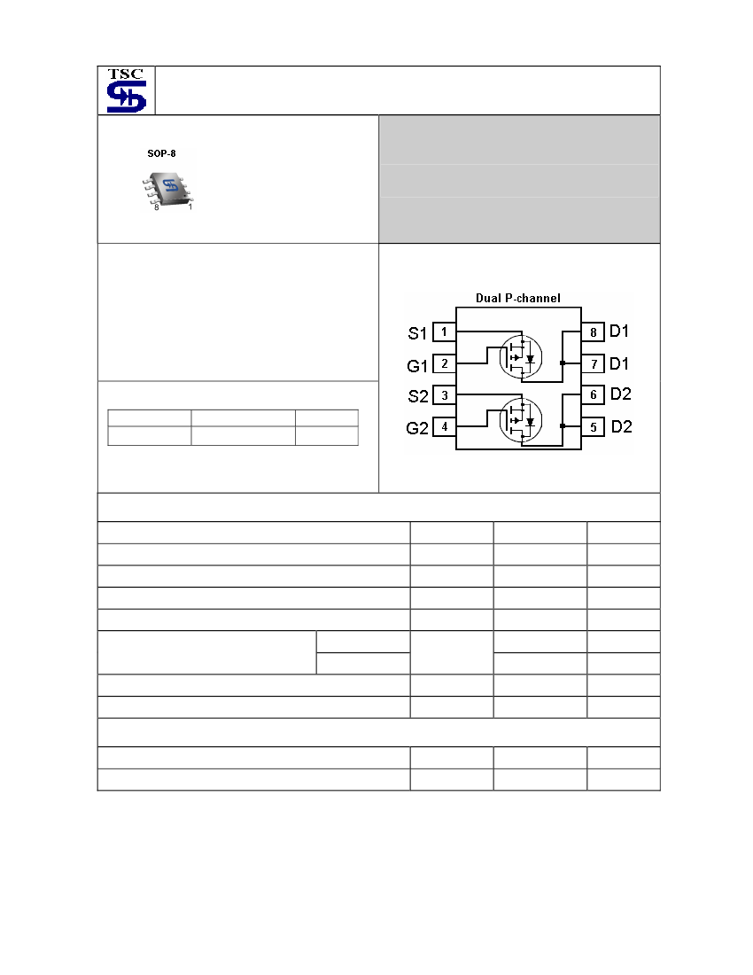


 1
1
 2
2
 3
3
