-
-

- 手機(jī)版
-

- 芯視頻 APP
-

- 微信公眾號(hào)
-

- 維庫(kù)官方抖音
-

- 微信頭條號(hào)
-
- |
-
- |
- |
- |

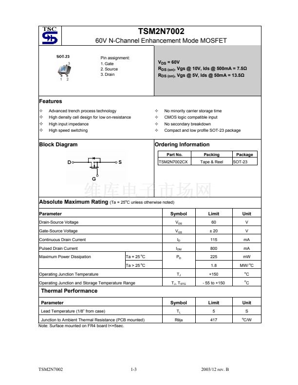
TSM2N7002CX
60V N-Channel Enhancement Mode MOSFET
129.84KB
3頁(yè)
TSC
掃碼查看芯片數(shù)據(jù)手冊(cè)
上傳產(chǎn)品規(guī)格書(shū)
Taiwan Semiconductor
MOSFET
N-Channel
60 V
+/- 20 V
0.3 A
7500 mOhms
Single
+ 150 C
SMD/SMT
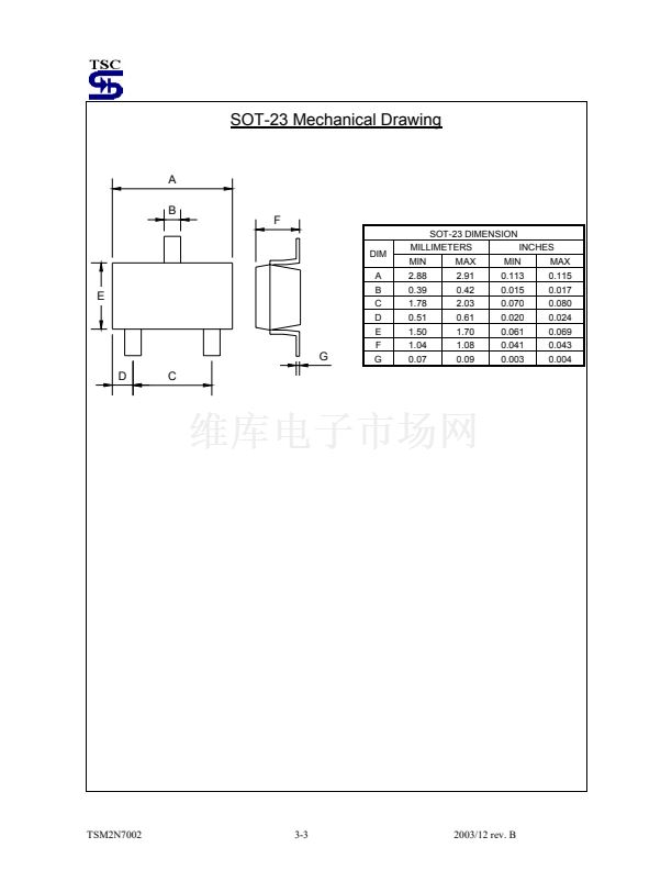
SOT-23-3
Reel
- 55 C
350 mW
3000
RF


聯(lián)系人:
聯(lián)系方式:

 1
1
 2
2
 3
3
