10-bit resolution.
2 GSPS sampling rate.
3 GHz full power input bandwidth.
0.2 dB (from DC up to 1.5 GHz).
Very low input VSWR : 1.15 max from DC to 2GHz (packaged device).
Power consumption : 4.6 W.
= 700 MHz [-1dBFS].
= 1950 MHz [-1dBFS].
= 950 MHz [-1dBFS].
LSB.
500 mVpp differential 100鈩?or single-ended 50鈩?/div>
(鹵1 %)
analog inputs.
Differential 100鈩?or single-ended 50鈩?ECL compatible clock inputs.
ECL or LVDS output compatibility.
50鈩?differential outputs with common mode independent on temperature.
Data ready output with asynchronous reset.
Out-of-Range output bit.
Gray or Binary selectable output data ; NRZ output mode.
Pattern generator output (for acquisition system monitoring).
ADC gain adjust.
Sampling delay adjust.
Offset control capability.
Radiation tolerance oriented design (more than 100Krad (Si) expected).
ADC 10-bit 2 Gsps
Converter
TS83102G0
APPLICATION
!
!
!
!
!
!
Direct RF down conversion.
Wide band satellite receiver.
High speed instrumentation.
High speed acquisition systems.
High energy physics.
Automatic test equipment.
1/ CBGA148 down
TS83102G0CGL
2/ Die form : JTS83102G0
3/ Hermetic ceramic package :
to be defined on request
4/ DMUX 10 bit 1:4/1:8 2Gsps
TS81102G0 :
Companion device available
5/ CBGA package Evaluation
Board TSEV83102G0GL
SCREENING
!
!
Standard die flow
Package Temperature range : To be defined
DESCRIPTION
The TS83102G0 is a monolithic 10-bit analog-to-digital converter, designed for digitizing
wide bandwidth analog signals at very high sampling rates of up to 2 Gsps.
The TS83102G0 is using an innovative architecture, including an on-chip Sample and
Hold (S/H), and is fabricated with an advanced high speed bipolar SiGe heterojunction
process, featuring 75GHz cutoff frequency.
The 3 GHz full power input bandwidth and the band flatness performances enables the
digitizing of high IF and large bandwidth signals.
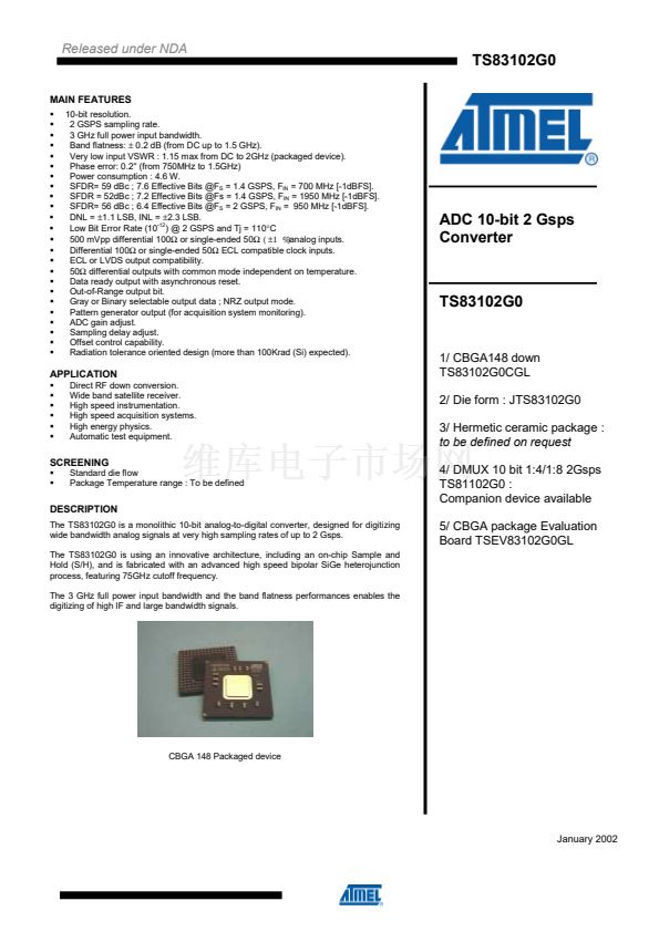
CBGA 148 Packaged device
January 2002


 1
1
