TS13002
High Voltage NPN Transistor
BV
CEO
= 400V
BV
CBO
= 700V
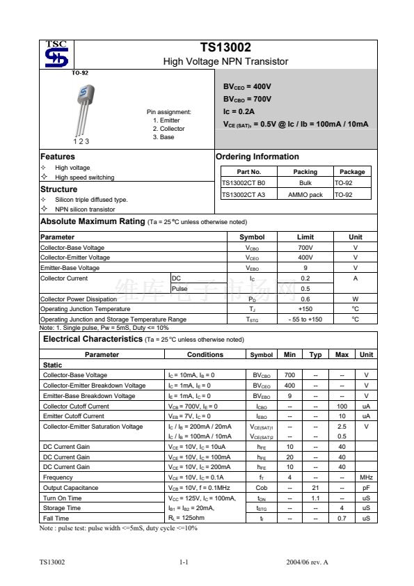
Pin assignment:
1. Emitter
2. Collector
3. Base
Ic = 0.2A
V
CE (SAT)
, = 0.5V @ Ic / Ib = 100mA / 10mA
Features
High voltage
.
High speed switching
Ordering Information
Part No.
TS13002CT B0
TS13002CT A3
Packing
Bulk
AMMO pack
Package
TO-92
TO-92
Structure
Silicon triple diffused type.
NPN silicon transistor
Absolute Maximum Rating
(Ta = 25
o
C unless otherwise noted)
Parameter
Collector-Base Voltage
Collector-Emitter Voltage
Emitter-Base Voltage
Collector Current
Collector Power Dissipation
Operating Junction Temperature
Operating Junction and Storage Temperature Range
Note: 1. Single pulse, Pw = 5mS, Duty <= 10%
DC
Pulse
P
D
T
J
T
STG
Symbol
V
CBO
V
CEO
V
EBO
I
C
Limit
700V
400V
9
0.2
0.5
0.6
+150
- 55 to +150
Unit
V
V
V
A
W
o
o
C
C
Electrical Characteristics
(Ta = 25
o
C unless otherwise noted)
Parameter
Static
Collector-Base Voltage
Collector-Emitter Breakdown Voltage
Emitter-Base Breakdown Voltage
Collector Cutoff Current
Emitter Cutoff Current
Collector-Emitter Saturation Voltage
DC Current Gain
DC Current Gain
DC Current Gain
Frequency
Output Capacitance
Turn On Time
Storage Time
Fall Time
I
C
= 10mA, I
B
= 0
I
C
= 1mA, I
E
= 0
I
E
= 1mA, I
C
= 0
V
CB
= 700V, I
E
= 0
V
EB
= 7V, I
C
= 0
I
C
/ I
B
= 200mA / 20mA
I
C
/ I
B
= 100mA / 10mA
V
CE
= 10V, I
C
= 10uA
V
CE
= 10V, I
C
= 100mA
V
CE
= 10V, I
C
= 200mA
V
CE
= 10V, I
C
= 0.1A
V
CB
= 10V, f = 0.1MHz
V
CC
= 125V, I
C
= 100mA,
I
B1
= I
B2
= 20mA,
R
L
= 125ohm
BV
CBO
BV
CEO
BV
EBO
I
CBO
I
EBO
V
CE(SAT)1
V
CE(SAT)2
h
FE
h
FE
h
FE
f
T
Cob
t
ON
t
STG
t
f
700
400
9
--
--
--
--
10
20
10
4
--
--
--
--
--
--
--
--
--
--
--
--
--
--
--
21
1.1
--
--
--
--
--
100
10
2.5
0.5
40
40
40
--
--
--
4
0.7
MHz
pF
uS
uS
uS
V
V
V
uA
uA
V
Conditions
Symbol
Min
Typ
Max
Unit
Note : pulse test: pulse width <=5mS, duty cycle <=10%
TS13002
1-1
2004/06 rev. A


 1
1
 2
2
