TS12N30CS 鈥?30V Single N-Channel 4.5V Specified AceFET鈩?/div>
General Description
Taiwan Semiconductor鈥檚 new low cost,
state of the art AceFET鈩?lateral MOSFET
process technology in chipscale
bondwireless packaging minimizes PCB
space and R
DS(ON)
plus provides an ultra-
low Qg X R
DS(ON)
figure of merit.
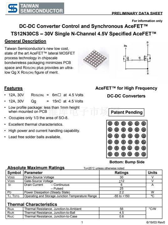
Ds
D
G
S
Features
鈥?12A, 30V
鈥?12A, 30V
R
DS(ON)
= 6m
Qg
at 4.5 Volts
= 15nC at 4.5 Volts
AceFET鈩?for High Frequency
DC-DC Converters
鈥?Low profile package: less than 1mm height
when mounted on PCB
鈥?Occupies only 1/3 the area of SO-8.
鈥?Excellent thermal characteristics.
鈥?High power and current handling capability.
鈥?Lead free solder balls available.
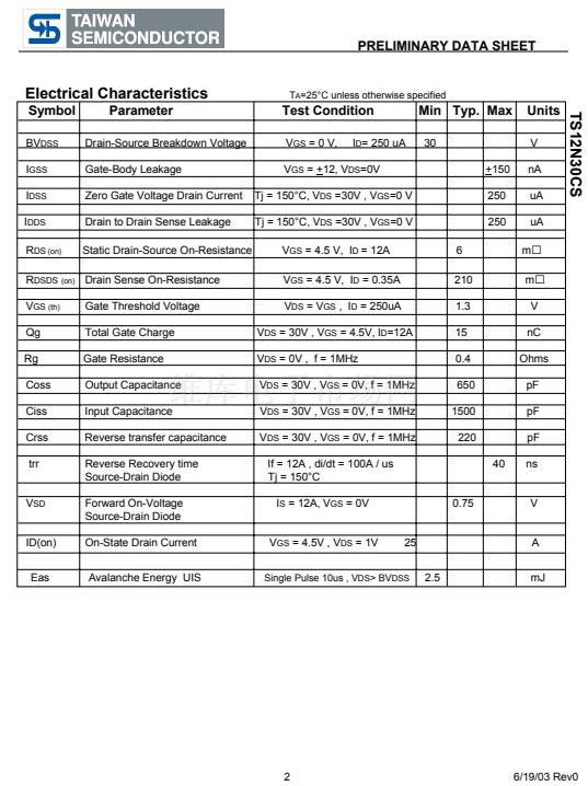
Patent Pending
D
S
D
S
D
S
S
D
S
D
S
D
D
S
D
S
D
S
S
D
S
D
S
D
D
S
D
S
D
S
S
D
G
D
s
S
D
Bottom: Bump Side
Absolute Maximum Ratings
Symbol Parameter
V
DSS
V
GSS
I
D
P
D
T
J
, T
STG
T
A
=25擄C unless otherwise noted
Ratings
30
+12
6
25
2.2
-55 to +150
Units
V
V
A
W
潞C
Drain-Source Voltage
Gate-Source Voltage
Drain Current
鈥?Continuous
鈥?Pulsed
Power Dissipation (Steady State)
Operating and Storage Junction Temperature Range
Thermal Characteristics
R
胃JA
R
胃JR
R
胃JC
Thermal Resistance, Junction-to-Ambient
Thermal Resistance, Junction-to-Ball
Thermal Resistance, Junction-to-Case
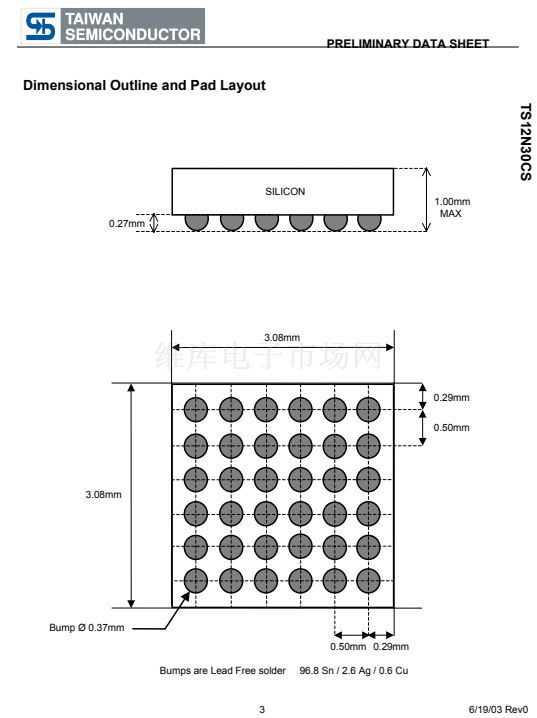
1
56
4.5
0.6
擄C/W
6/19/03 Rev0


 1
1
 2
2
 3
3
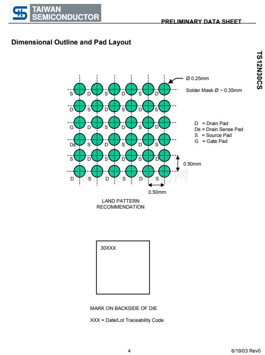 4
4
