TRF8010
900-MHz RF TRANSMIT DRIVER
SLWS031B 鈥?JULY 1996鈥?REVISED MAY 1997
D
D
D
D
D
D
D
D
D
Operates from 3.6-V and 4.8-V Power
Supplies for AMPS/NADC and GSM
Applications Respectively
Unconditionally Stable
Wide UHF Frequency Range
800 MHz to 1000 MHz
21 dBm and 23 dBm Typical Output Power
in AMPS/NADC and GSM Applications
Respectively
Linear Ramp Control
Transmit Enable/Disable Control
Advanced BiCMOS Processing Technology
for Low-Power Consumption, High
Efficiency, and Highly Linear Operation
Minimum of External Components
Required for Operation
Surface-Mount Thermally Enhanced
Package for Extremely Small Circuit
Footprint
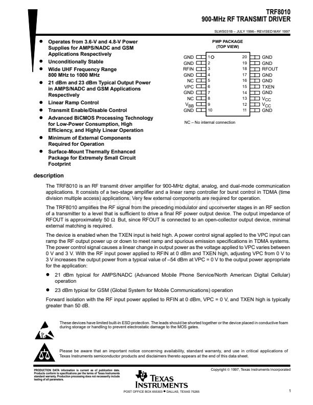
PWP PACKAGE
(TOP VIEW)
GND
GND
RFIN
GND
NC
VPC
GND
NC
V
BB
GND
1
2
3
4
5
6
7
8
9
10
20
19
18
17
16
15
14
13
12
11
GND
GND
RFOUT
GND
GND
TXEN
GND
V
CC
V
CC
GND
NC 鈥?No internal connection
description
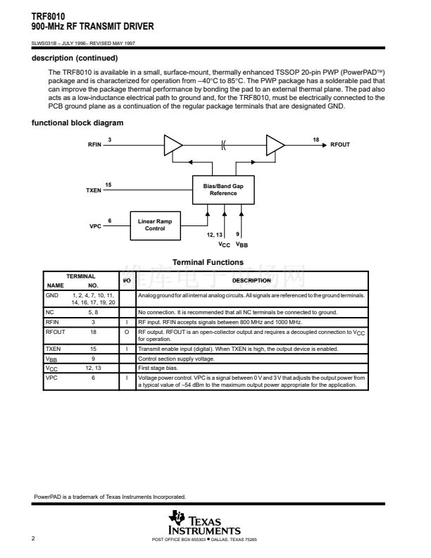
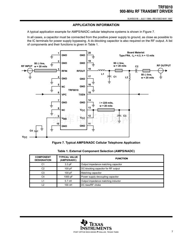
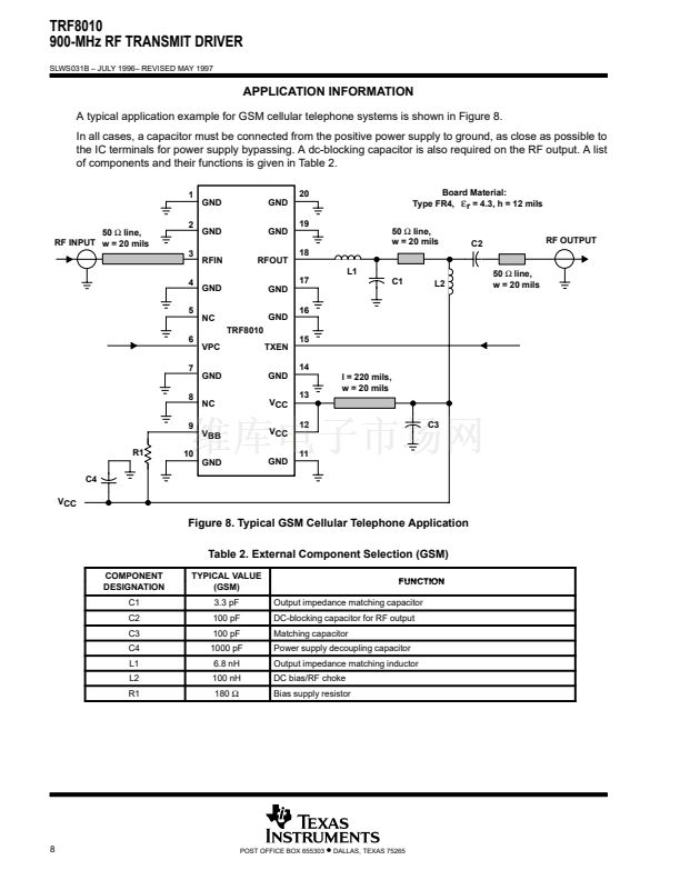
The TRF8010 is an RF transmit driver amplifier for 900-MHz digital, analog, and dual-mode communication
applications. It consists of a two-stage amplifier and a linear ramp controller for burst control in TDMA (time
division multiple access) applications. Very few external components are required for operation.
The TRF8010 amplifies the RF signal from the preceding modulator and upconverter stages in an RF section
of a transmitter to a level that is sufficient to drive a final RF power output device. The output impedance of
RFOUT is approximately 50
鈩?
But, since RFOUT is connected to an open-collector output device, minimal
external matching is required.
The device is enabled when the TXEN input is held high. A power control signal applied to the VPC input can
ramp the RF output power up or down to meet ramp and spurious emission specifications in TDMA systems.
The power control signal causes a linear change in output power as the voltage applied to VPC varies between
0 V and 3 V. With the RF input power applied to RFIN at 0 dBm and TXEN high, adjusting VPC from 0 V to
3 V increases the output power from a typical value of 鈥?4 dBm at VPC = 0 V to the output power appropriate
for the application:
D
D
21 dBm typical for AMPS/NADC (Advanced Mobile Phone Service/North American Digital Cellular)
operation
23 dBm typical for GSM (Global System for Mobile Communications) operation
Forward isolation with the RF input power applied to RFIN at 0 dBm, VPC = 0 V, and TXEN high is typically
greater than 50 dB.
These devices have limited built-in ESD protection. The leads should be shorted together or the device placed in conductive foam
during storage or handling to prevent electrostatic damage to the MOS gates.
Please be aware that an important notice concerning availability, standard warranty, and use in critical applications of
Texas Instruments semiconductor products and disclaimers thereto appears at the end of this data sheet.
Copyright
漏
1997, Texas Instruments Incorporated
PRODUCTION DATA information is current as of publication date.
Products conform to specifications per the terms of Texas Instruments
standard warranty. Production processing does not necessarily include
testing of all parameters.
POST OFFICE BOX 655303
鈥?/div>
DALLAS, TEXAS 75265
1


 1
1
 2
2
 3
3
 4
4
 5
5
 6
6
 7
7
 8
8
 9
9
 10
10
