TRF5001
GPS RF RECEIVER
SLWS084 鈥?DECEMBER 2000
D
Complete L1-Band Global Postioning
D
D
D
D
D
D
D
D
System (GPS) RF Receiver
2.7-V to 3.3-V Operation
Low Current Consumption, 49 mA Typical
at 2.7 V
Integrated Voltage-Controlled Oscillator
(VCO) Tank Circuit
Compatible With Cellular Phone
Environment While Transmitter Is Active
Programmable Sleep Mode for Extended
Standby Time
Integrated Low Noise Amplifier (LNA) and
Image Reject Mixer Front-End With Typical
Cascaded Noise Figure of 2.9 dB
Integrated Phase-Locked Loop (PLL)
4-Bit Analog-To-Digital Converter (ADC)
With Programmable Automatic Gain
Control (AGC) for Improved GPS Receiver
Sensitivity
Operating Temperature Range: 鈥?0擄C to
85擄C
Code Division Multiple Access/ Time-
Division Multiple Access
(CDMA/TDMA/GSM) System Clock-
Compatible Synthesizer
Image-Reject Architecture for Reduced
Parts Count and Page Control Block (PCB)
Real Estate Requirements
3-Wire Serial Interface and Single Blanking
Mode Control Terminal
1
A
B
C
D
E
F
G
H
J
2
GQE PACKAGE
(TOP VIEW)
3
4
5
6
7
8
9
D
D
D
Digital CMOS Compatible Inputs/Outputs
D
User-Selected Internal/External Sampling
D
D
Clock for ADC
RF BiCMOS technology with ESD
Protection to 2000 V HBM (non-RF Pins)
Chip Scale Package (CSP) 5 mm x 5 mm
D
D
description
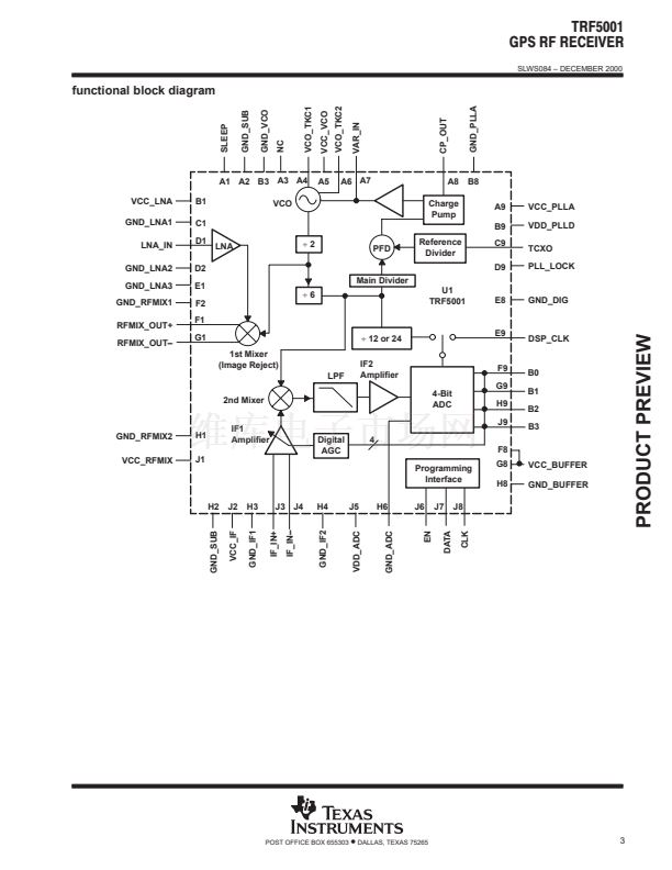
The TRF5001 device is a dual down-conversion receiver that is compatible with cellular terminals while the
transmitter is active. The TRF5001 device includes an integrated low-noise amplifier and mixer, a
fixed-frequency synthesizer to generate both first and second local oscillator frequencies, and a four-bit ADC
for use in GPS applications requiring exceptional sensitivity, such as E-911. By using only the most significant
bit (MSB), the TRF5001 device can be mated to more conventional baseband processors requiring only single
bit resolution. The typical first intermediate frequency is 222.54 MHz with a final intermediate frequency into the
ADC of 2.94 MHz. An external or internal sampling clock can be selected for custom use of the TRF5001 device,
as long as the Nyquist sampling rate is satisfied.
These devices have limited built-in ESD protection. The leads should be shorted together or the device placed in conductive foam
during storage or handling to prevent electrostatic damage to the gates.
Please be aware that an important notice concerning availability, standard warranty, and use in critical applications of
Texas Instruments semiconductor products and disclaimers thereto appears at the end of this data sheet.
TI is a trademark of Texas Instruments Incorporated.
PRODUCT PREVIEW information concerns products in the formative or
design phase of development. Characteristic data and other
specifications are design goals. Texas Instruments reserves the right to
change or discontinue these products without notice.
Copyright
漏
2000, Texas Instruments Incorporated
POST OFFICE BOX 655303
鈥?/div>
DALLAS, TEXAS 75265
1
PRODUCT PREVIEW


 1
1
 2
2
 3
3
 4
4
 5
5
 6
6
 7
7
 8
8
 9
9
 10
10
 11
11
 12
12
 13
13
 14
14
 15
15
 16
16
 17
17
 18
18
 19
19
