TPS5615, TPS5618, TPS5625, TPS5633
SYNCHRONOUS-BUCK HYSTERETIC REGULATOR CONTROLLER
SLVS177B 鈥?SEPTEMBER 1998 鈥?REVISED JULY 2000
D
D
D
D
D
D
D
D
D
D
鹵1%
Reference Over Full Operating
Temperature Range
Synchronous Rectifier Driver for >90%
Efficiency
Fixed Output Voltage Options of 1.5 V,
1.8 V, 2.5 V, and 3.3 V
User-Selectable Hysteretic-Type Control
Low Supply Current . . . 3 mA Typ
11.4-V to 13-V Input Voltage Range, V
CC
Power Good Output
Programmable Soft-Start
Overvoltage/Overcurrent Protection
Active Deadtime Control
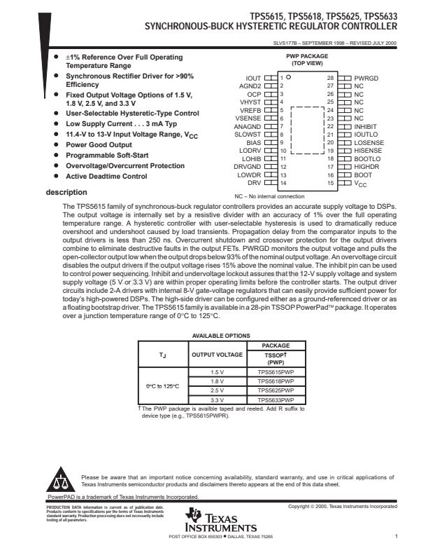
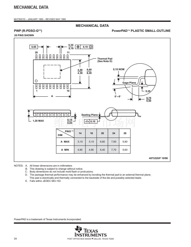
PWP PACKAGE
(TOP VIEW)
IOUT
AGND2
OCP
VHYST
VREFB
VSENSE
ANAGND
SLOWST
BIAS
LODRV
LOHIB
DRVGND
LOWDR
DRV
1
2
3
4
5
6
7
8
9
10
11
12
13
14
28
27
26
25
24
23
22
21
20
19
18
17
16
15
PWRGD
NC
NC
NC
NC
NC
INHIBIT
IOUTLO
LOSENSE
HISENSE
BOOTLO
HIGHDR
BOOT
V
CC
description
NC 鈥?No internal connection
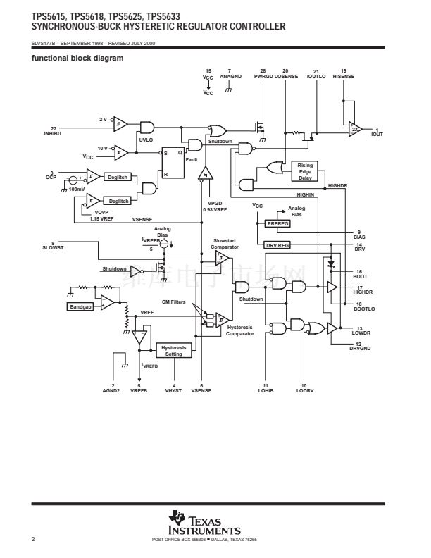
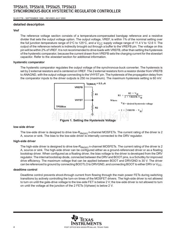
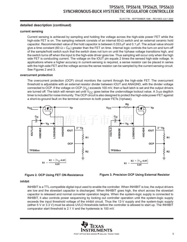
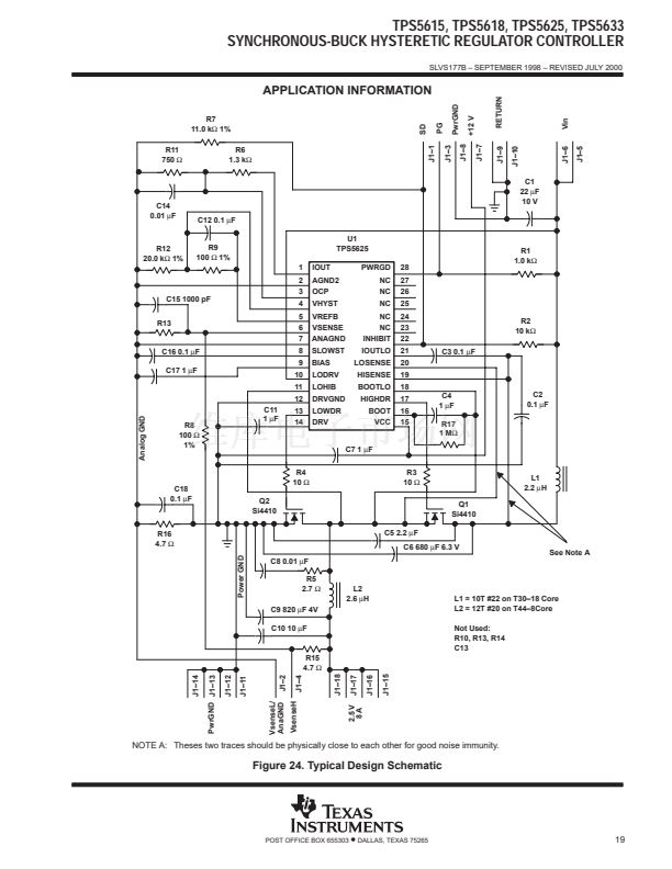
The TPS5615 family of synchronous-buck regulator controllers provides an accurate supply voltage to DSPs.
The output voltage is internally set by a resistive divider with an accuracy of 1% over the full operating
temperature range. A hysteretic controller with user-selectable hysteresis is used to dramatically reduce
overshoot and undershoot caused by load transients. Propagation delay from the comparator inputs to the
output drivers is less than 250 ns. Overcurrent shutdown and crossover protection for the output drivers
combine to eliminate destructive faults in the output FETs. PWRGD monitors the output voltage and pulls the
open-collector output low when the output drops below 93% of the nominal output voltage. An overvoltage circuit
disables the output drivers if the output voltage rises 15% above the nominal value. The inhibit pin can be used
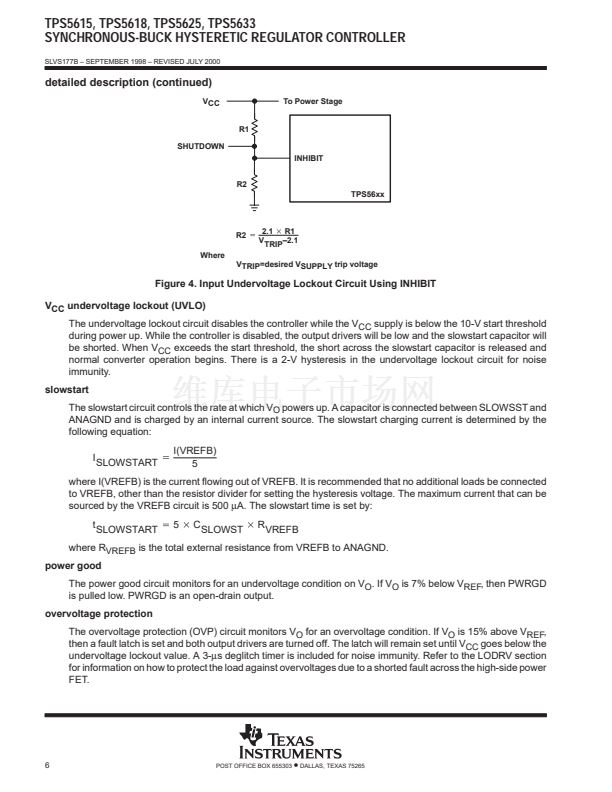
to control power sequencing. Inhibit and undervoltage lockout assures that the 12-V supply voltage and system
supply voltage (5 V or 3.3 V) are within proper operating limits before the controller starts. The output driver
circuits include 2-A drivers with internal 8-V gate-voltage regulators that can easily provide sufficient power for
today鈥檚 high-powered DSPs. The high-side driver can be configured either as a ground-referenced driver or as
a floating bootstrap driver. The TPS5615 family is available in a 28-pin TSSOP PowerPad鈩?package. It operates
over a junction temperature range of 0擄C to 125擄C.
AVAILABLE OPTIONS
TJ
OUTPUT VOLTAGE
1.5 V
0擄C to 125擄C
1.8 V
2.5 V
PACKAGE
TSSOP鈥?/div>
(PWP)
TPS5615PWP
TPS5618PWP
TPS5625PWP
3.3 V
TPS5633PWP
鈥?The PWP package is availble taped and reeled. Add R suffix to
device type (e.g., TPS5615PWPR).
Please be aware that an important notice concerning availability, standard warranty, and use in critical applications of
Texas Instruments semiconductor products and disclaimers thereto appears at the end of this data sheet.
PowerPAD is a trademark of Texas Instruments Incorporated.
PRODUCTION DATA information is current as of publication date.
Products conform to specifications per the terms of Texas Instruments
standard warranty. Production processing does not necessarily include
testing of all parameters.
Copyright
漏
2000, Texas Instruments Incorporated
POST OFFICE BOX 655303
鈥?/div>
DALLAS, TEXAS 75265
1


 1
1
 2
2
 3
3
 4
4
 5
5
 6
6
 7
7
 8
8
 9
9
 10
10
 11
11
 12
12
 13
13
 14
14
 15
15
 16
16
 17
17
 18
18
 19
19
 20
20
 21
21
 22
22
 23
23
 24
24
 25
25
 26
26
