Siliconix
TN0201T
N Channel Enhancement Mode MOS Transistor
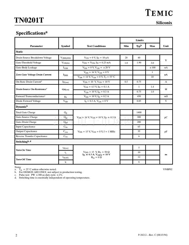
Product Summary
V
(BR)DSS
Min (V)
20
r
DS(on)
Max (W)
1.0 @ V
GS
= 10 V
1.4 @ V
GS
= 4.5 V
V
GS(th)
(V)
1.0 to 3.0
I
D
(A)
0.3
Features
D
D
D
D
D
Low On Resistance: 0.75
W
Low Threshold: <1.75 V
Low Input Capacitance: 65 pF
Fast Switching Speed: 15 ns
Low Input and Output Leakage
Benefits
D
D
D
D
D
Low Offset Voltage
Low Voltage Operation
Easily Driven Without Buffer
High Speed Circuits
Low Error Voltage
Applications
D
Direct Logic Level Interface: TTL/CMOS
D
Drivers: Relays, Solenoids, Lamps, Hammers,
Displays, Memories, Transistors, etc.
D
Battery Operated Systems
D
Solid State Relays
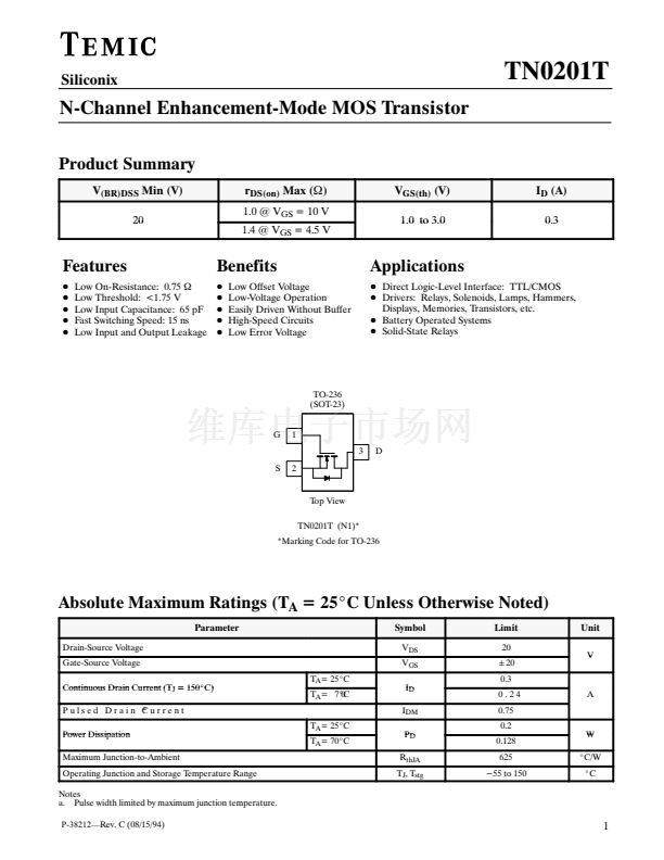
TO 236
(SOT 23)
G
S
1
3
2
D
Top View
TN0201T (N1)*
*Marking Code for TO 236
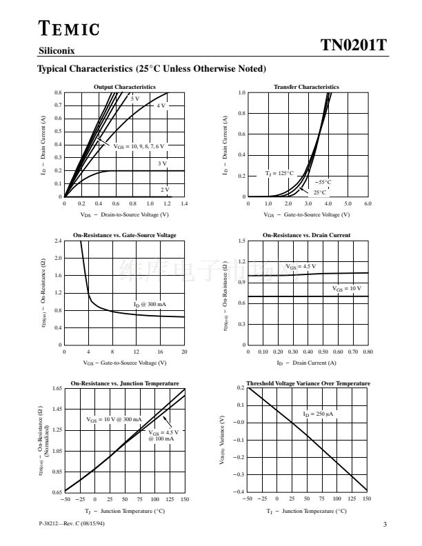
Absolute Maximum Ratings (T
A
= 25_C Unless Otherwise Noted)
Parameter
Drain Source Voltage
Gate Source Voltage
Continuous Drain Current (T
J
= 150_C)
a
Pulsed Drain Current
Symbol
V
DS
V
GS
T
A
= 25_C
T
A
= 7
_C
0
T
A
= 25_C
T
A
= 70_C
I
D
I
DM
P
D
R
thJA
T
J
, T
stg
Limit
20
"20
0.3
0.24
0.75
0.2
0.128
625
-55 to 150
Unit
V
A
Power Dissipation
Maximum Junction to Ambient
Operating Junction and Storage Temperature Range
Notes
a. Pulse width limited by maximum junction temperature.
P-38212鈥擱ev.
C (08/15/94)
W
_C/W
_C
1


 1
1
 2
2
 3
3
 4
4
