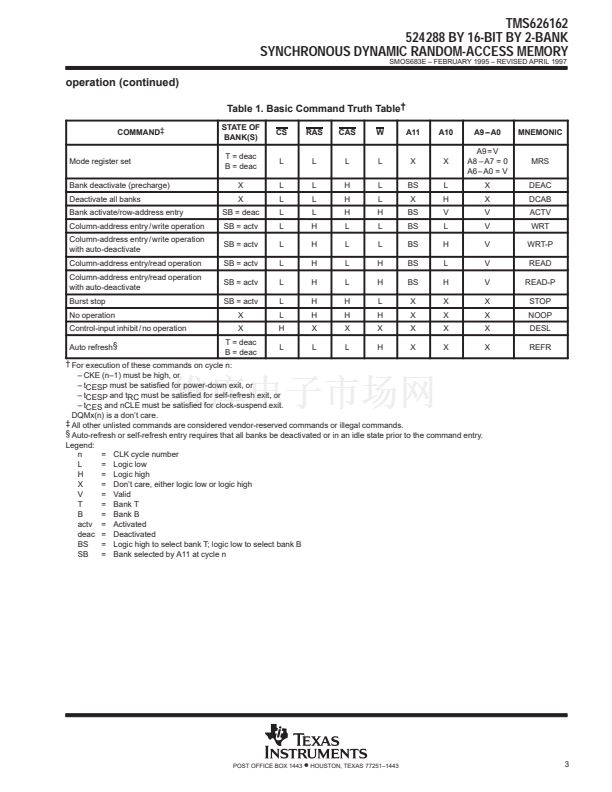
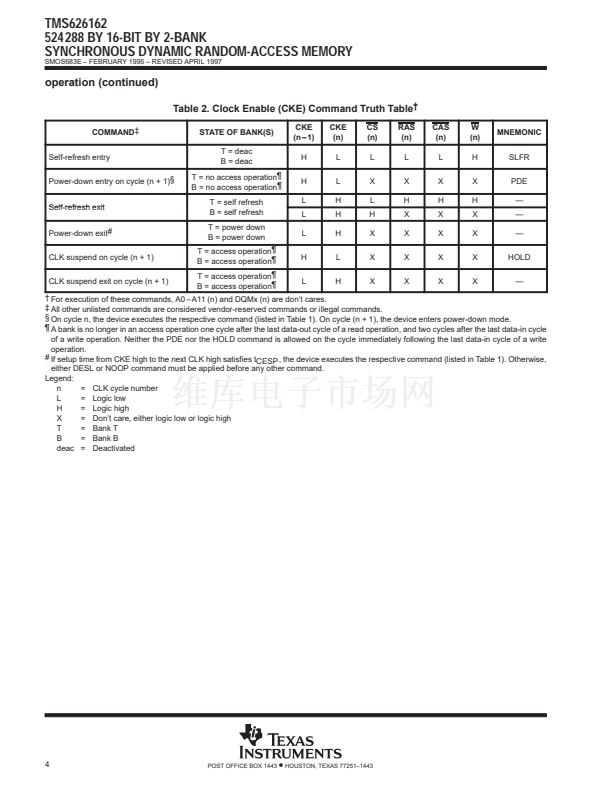
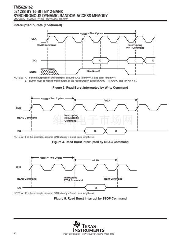
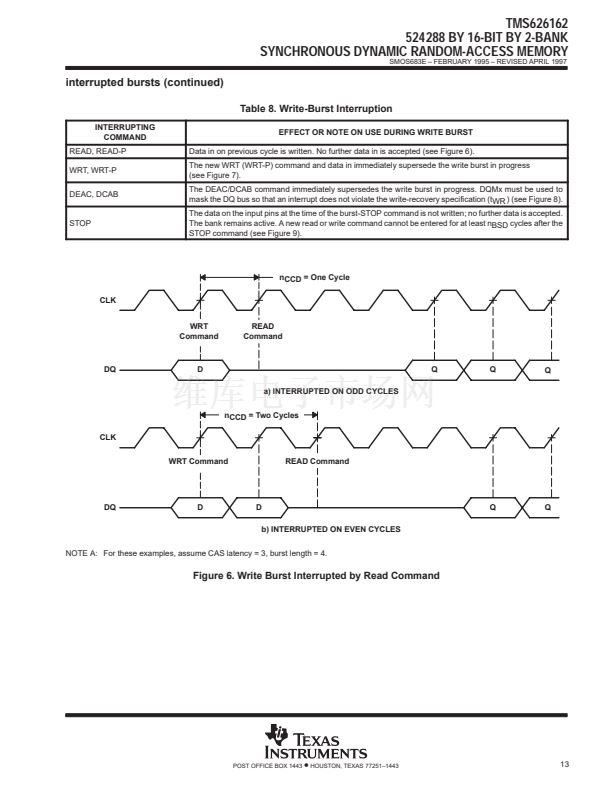
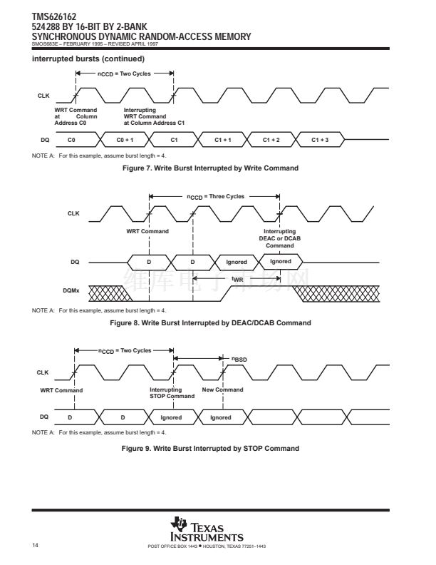
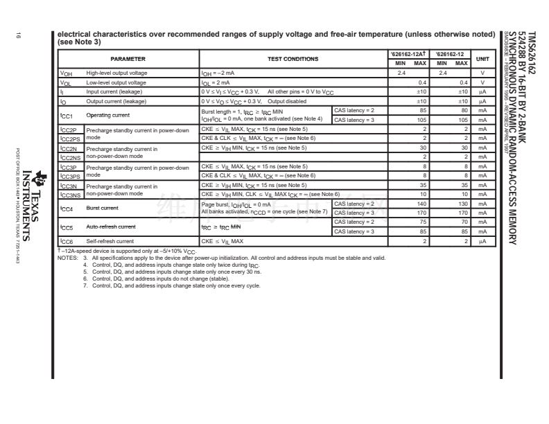
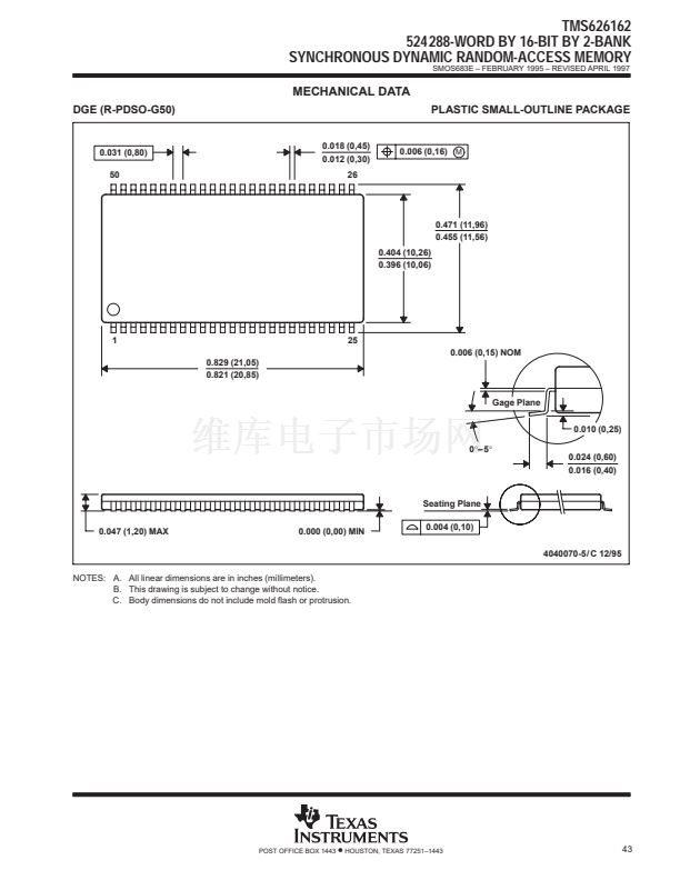
TMS626162
524288 BY 16-BIT BY 2-BANK
SYNCHRONOUS DYNAMIC RANDOM-ACCESS MEMORY
SMOS683E 鈥?FEBRUARY 1995 鈥?REVISED APRIL 1997
D
D
D
D
D
D
D
D
D
D
D
D
D
D
D
D
Organization . . . 512K
脳
16
脳
2 Banks
3.3-V Power Supply (鹵 10% Tolerance)
Two Banks for On-Chip Interleaving
(Gapless Accesses)
High Bandwidth 鈥?Up to 83-MHz Data Rates
CAS Latency (CL) Programmable to 2 or 3
Cycles From Column-Address Entry
Burst Sequence Programmable to Serial or
Interleave
Burst Length Programmable to 1, 2, 4, 8, or
Full Page
Chip Select and Clock Enable for
Enhanced-System Interfacing
Cycle-by-Cycle DQ-Bus Mask Capability
With Upper and Lower Byte Control
Auto-Refresh and Self-Refresh Capability
4K Refresh (Total for Both Banks)
High-Speed, Low-Noise, Low-Voltage TTL
(LVTTL) Interface
Power-Down Mode
Compatible With JEDEC Standards
Pipeline Architecture
Temperature Ranges:
Operating, 0擄C to 70擄C
Storage, 鈥?55擄C to 150擄C
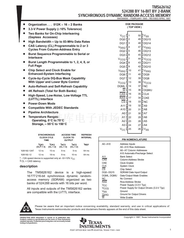
DGE PACKAGE
( TOP VIEW )
V
CC
DQ0
DQ1
V
SSQ
DQ2
DQ3
V
CCQ
DQ4
DQ5
V
SSQ
DQ6
DQ7
V
CCQ
DQML
W
CAS
RAS
CS
A11
A10
A0
A1
A2
A3
V
CC
1
2
3
4
5
6
7
8
9
10
11
12
13
14
15
16
17
18
19
20
21
22
23
24
25
50
49
48
47
46
45
44
43
42
41
40
39
38
37
36
35
34
33
32
31
30
29
28
27
26
V
SS
DQ15
DQ14
V
SSQ
DQ13
DQ12
V
CCQ
DQ11
DQ10
V
SSQ
DQ9
DQ8
V
CCQ
NC
DQMU
CLK
CKE
NC
A9
A8
A7
A6
A5
A4
V
SS
SYNCHRONOUS
CLOCK CYLE
TIME
tCK3
(CL鈥?= 3)
鈥?26162-12A鈥?/div>
鈥?26162-12
鈥?/div>
ACCESS TIME
CLOCK TO
OUTPUT
tAC3
(CL = 3)
9 ns
9 ns
tAC2
(CL = 2)
9 ns
10 ns
REFRESH
INTERVAL
tREF
64 ms
64 ms
PIN NOMENCLATURE
A0鈥揂10
Address Inputs
A0鈥揂10 Row Addresses
A0鈥揂7 Column Addresses
A10 Automatic-Precharge Select
Bank Select
Column-Address Strobe
Clock Enable
System Clock
Chip Select
SDRAM Data Input/Output
Data/Output Mask Enables
No Connect
Row-Address Strobe
Power Supply (3.3-V Typ)
Power Supply for Output Drivers (3.3-V Typ)
Ground
Ground for Output Drivers
Write Enable
tCK2
(CL = 2)
15 ns
18 ns
12 ns
12 ns
鈥?CL = CAS latency
鈥?2A speed device is supported only at 鈥?/+10% V
CC
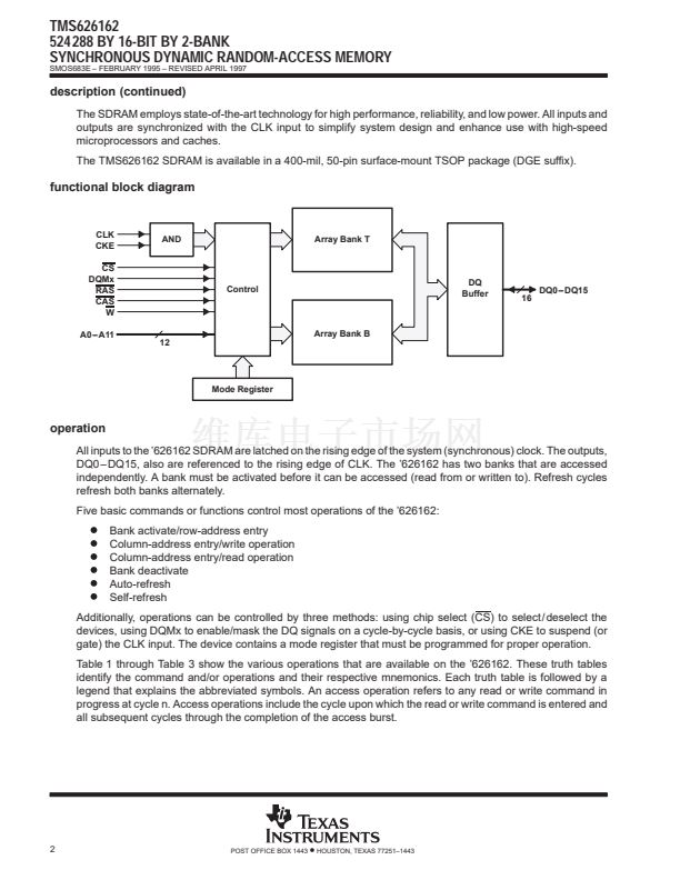
description
The TMS626162 device is a high-speed
16 777 216-bit synchronous dynamic random-
access memory (SDRAM) organized as two
banks of 524 288 words with 16 bits per word.
All inputs and outputs of the TMS626162 series
are compatible with the LVTTL interface.
A11
CAS
CKE
CLK
CS
DQ0鈥揇Q15
DQML, DQMU
NC
RAS
VCC
VCCQ
VSS
VSSQ
W
Please be aware that an important notice concerning availability, standard warranty, and use in critical applications of
Texas Instruments semiconductor products and disclaimers thereto appears at the end of this data sheet.
Copyright
漏
1997, Texas Instruments Incorporated
PRODUCTION DATA information is current as of publication date.
Products conform to specifications per the terms of Texas Instruments
standard warranty. Production processing does not necessarily include
testing of all parameters.
POST OFFICE BOX 1443
鈥?/div>
HOUSTON, TEXAS 77251鈥?443
1


 1
1
 2
2
 3
3
 4
4
 5
5
 6
6
 7
7
 8
8
 9
9
 10
10
 11
11
 12
12
 13
13
 14
14
 15
15
 16
16
 17
17
 18
18
 19
19
 20
20
 21
21
 22
22
 23
23
 24
24
 25
25
 26
26
 27
27
 28
28
 29
29
 30
30
 31
31
 32
32
 33
33
 34
34
 35
35
 36
36
 37
37
 38
38
 39
39
 40
40
 41
41
 42
42
 43
43
 44
44
