TMS28F033
4194304-BIT
SYNCHRONOUS FLASH MEMORY
SMJS833 鈥?NOVEMBER 1997
D
D
D
D
D
D
D
D
D
D
DQ26
DQ27
VDDE
VSSE
DQ28
DQ29
DQ30
DQ31
A鈥?
A0
A1
A2
13
14
15
16
17
18
19
20
21
22
23
24
52
51
50
49
48
47
46
45
44
43
42
41
25 26 27 28 29 30 31 32 33 34 35 36 37 38 39 40
DQ5
DQ4
VSSE
VDDE
DQ3
DQ2
DQ1
DQ0
NC
NC
NC
A16
VSSI
V PP
A10
A11
A3
A4
A5
A6
A7
A8
A9
A12
A14
V DDI
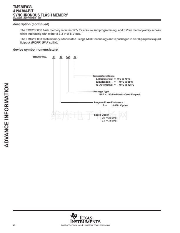
The TMS28F033 is the first synchronous
nonvolatile flash memory device to offer a
configurable burst interface to 16/32-bit microprocessors and microcontrollers operating at frequencies up to
40 MHz.
The TMS28F033 contains 4M bits of main memory that is user-configurable as either three or four
independently erasable blocks. In addition to the main memory array, there is a protected overlay memory block
that is normally hidden from the memory address map. The following table shows the three- and four-block
main-memory-array configurations for both 16-bit and 32-bit data bus widths.
Table 1. Memory Configurations
DATA BUS WIDTH
16 bits
32 bits
3-BLOCK MAIN ARRAY
32K, 160K, and 64K
16K, 80K, and 32K
4-BLOCK MAIN ARRAY
32K, 96K, 64K, and 64K
16K, 48K, 32K, and 32K
PROTECTED OVERLAY BLOCK
12K
6K
Embedded program and block-erase functions are fully automated by an on-chip write state machine (WSM),
which simplifies these operations and relieves the system microcontroller of these secondary tasks. WSM
status can be monitored by the on-chip status register to determine the progress of program/erase tasks.
Please be aware that an important notice concerning availability, standard warranty, and use in critical applications of
Texas Instruments semiconductor products and disclaimers thereto appears at the end of this data sheet.
Copyright
漏
1997, Texas Instruments Incorporated
ADVANCE INFORMATION concerns new products in the sampling or
preproduction phase of development. Characteristic data and other
specifications are subject to change without notice.
POST OFFICE BOX 1443
鈥?/div>
HOUSTON, TEXAS 77251鈥?443
A13
A15
description
1
ADVANCE INFORMATION
Organization
鈥?512K-Byte Main Array
鈥?24K-Byte Protected Overlay-Block
User-Defined x16 or x32 Data Bus
Read Transfer Data Rates Up to
100 MBytes / s at Bus Frequencies Up to
40 MHz
Burstable Pipelined Read Interface With
Programmable Latency, Length, and Order
10 000 Program / Erase Cycles
Three Temperature Ranges
鈥?Commercial . . . 0擄C to 70擄C
鈥?Extended . . . 鈥?40擄C to 85擄C
鈥?Automotive . . . 鈥?40擄C to 125擄C
80-Pin Plastic Quad Flatpack (PQFP)
(PAF Suffix)
Fully Automated On-Chip Erase and
Program Operations
Three Separate Voltage Supplies
鈥?I / O Supply 鈥?Configurable 3.3 V / 5 V
鈥?Read Supply 鈥?5 V
鈥?Programming Supply 鈥?12 V
All Inputs / Outputs TTL-Compatible
PAF
80-PIN PACKAGE
(T0P VIEW)
WORD/DIS
BAA/LRV
RY/BY
OE
80 79 78 77 76 75 74 73 72 71 70 69 68 67 66 65
DQ16
DQ17
DQ18
DQ19
VDDE
VSSE
DQ20
DQ21
DQ22
DQ23
DQ24
DQ25
1
2
3
4
5
6
7
8
9
10
11
12
V DDE
64
63
62
61
60
59
58
57
56
55
54
53
S/5IO
V DDI
V SSI
LBO
CLK
LBA
WR
WE
QV
RP
E
DQ15
DQ14
DQ13
DQ12
VSSE
VDDE
DQ11
DQ10
DQ9
DQ8
DQ7
DQ6


 1
1
 2
2
 3
3
 4
4
 5
5
 6
6
 7
7
 8
8
 9
9
 10
10
 11
11
 12
12
 13
13
 14
14
 15
15
 16
16
 17
17
 18
18
 19
19
 20
20
 21
21
 22
22
 23
23
 24
24
 25
25
 26
26
 27
27
 28
28
 29
29
 30
30
 31
31
 32
32
 33
33
 34
34
 35
35
 36
36
 37
37
 38
38
 39
39
 40
40
 41
41
 42
42
 43
43
 44
44
 45
45
 46
46
 47
47
 48
48
 49
49
 50
50
 51
51
 52
52
