TIS73 / TIS74
TIS73
TIS74
G
S
TO-92
D
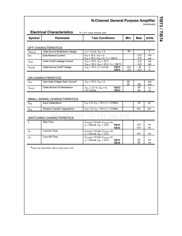
N-Channel General Purpose Amplifier
This device is designed for low level analog switching, sample
and hold circuits and chopper stabalized amplifiers. Sourced from
Process 54.
Absolute Maximum Ratings*
Symbol
V
DG
V
GS
I
GF
T
J
, T
stg
Drain-Gate Voltage
Gate-Source Voltage
Forward Gate Current
TA = 25擄C unless otherwise noted
Parameter
Value
30
- 30
10
-55 to +150
Units
V
V
mA
擄C
Operating and Storage Junction Temperature Range
*
These ratings are limiting values above which the serviceability of any semiconductor device may be impaired.
NOTES:
1)
These ratings are based on a maximum junction temperature of 150 degrees C.
2)
These are steady state limits. The factory should be consulted on applications involving pulsed or low duty cycle operations.
Thermal Characteristics
Symbol
P
D
R
胃
JC
R
胃JA
TA = 25擄C unless otherwise noted
Characteristic
Total Device Dissipation
Derate above 25擄C
Thermal Resistance, Junction to Case
Thermal Resistance, Junction to Ambient
Max
TIS73 / TIS74
625
5.0
83.3
200
Units
mW
mW/擄C
擄C/W
擄C/W
漏1997
Fairchild Semiconductor Corporation


 1
1
 2
2
 3
3
 4
4
