TC7PA04FU
TOSHIBA CMOS Digital Integrated Circuit Silicon Monolithic
TC7PA04FU
Dual Inverter with 3.6 V Tolerant Input and Output
Features
路
路
Operating voltage range: V
CC
= 1.8~3.6 V
High-speed operation: t
pd
= 2.8 ns (max) at V
CC
= 3.0~3.6 V
t
pd
= 3.7 ns (max) at V
CC
= 2.3~2.7 V
t
pd
= 7.4 ns (max) at V
CC
= 1.8 V
路
High-level output current:
I
OH
/I
OL
= 鹵24 mA (min) at V
CC
= 3.0 V
I
OH
/I
OL
= 鹵18 mA (min) at V
CC
= 2.3 V
I
OH
/I
OL
= 鹵6 mA (min) at V
CC
= 1.8 V
路
路
路
路
High latch-up immunity: 鹵300 mA
High ESD: Higher than or equal to 鹵200 V (JEITA)
Higher than or equal to 鹵2000 V (MIL)
3.6-V tolerant function and power-down protection provided on all inputs and outputs
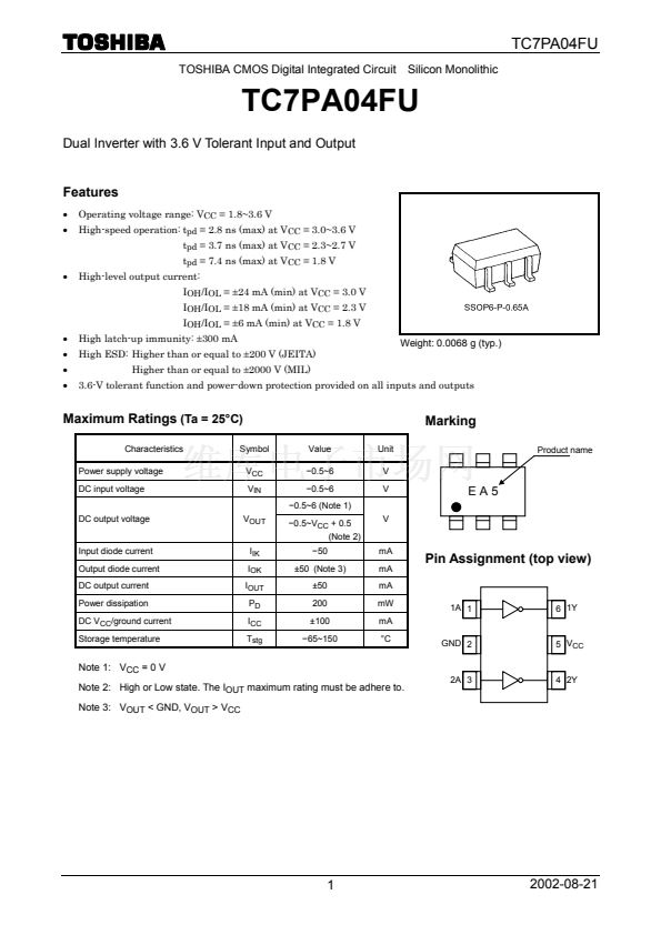
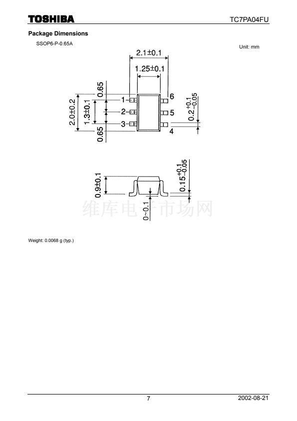
Weight: 0.0068 g (typ.)
Maximum Ratings
(Ta = 25擄C)
Characteristics
Power supply voltage
DC input voltage
DC output voltage
Input diode current
Output diode current
DC output current
Power dissipation
DC V
CC
/ground current
Storage temperature
Symbol
V
CC
V
IN
V
OUT
I
IK
I
OK
I
OUT
P
D
I
CC
T
stg
Value
鈭?.5~6
鈭?.5~6
鈭?.5~6
(Note 1)
鈭?.5~V
CC
+ 0.5
(Note 2)
鈭?0
鹵50 (Note 3)
鹵50
200
鹵100
鈭?5~150
V
mA
mA
mA
mW
mA
擄C
Unit
V
V
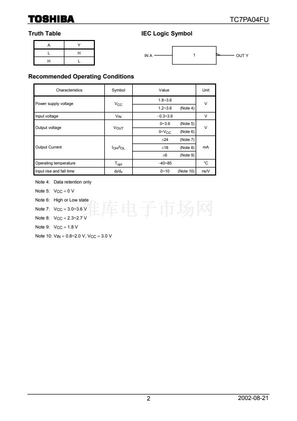
Marking
Product name
EA5
Pin Assignment (top view)
1A 1
6 1Y
GND 2
5 V
CC
Note 1: V
CC
= 0 V
Note 2: High or Low state. The I
OUT
maximum rating must be adhere to.
Note 3: V
OUT
< GND, V
OUT
> V
CC
2A 3
4 2Y
1
2002-08-21


 1
1
 2
2
 3
3
 4
4
 5
5
 6
6
 7
7
 8
8
