TC58DVG02A1FT00
TENTATIVE
TOSHIBA MOS DIGITAL INTEGRATED CIRCUIT SILICON GATE CMOS
2
1-GBIT (128M 8 BITS) CMOS NAND E PROM
DESCRIPTION
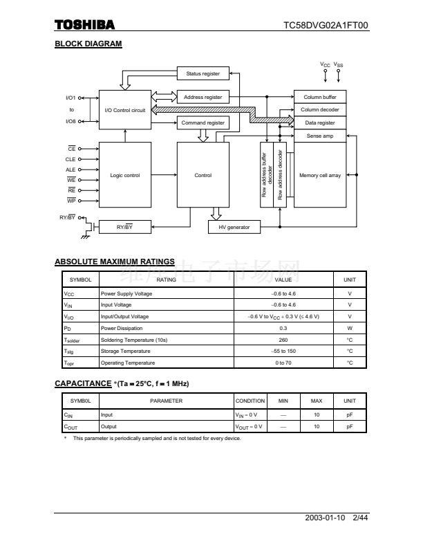
The TC58DVG02A1 is a single 3.3 V 1-Gbit (1,107,296,256) bit NAND Electrically Erasable and Programmable
Read-Only Memory (NAND E
2
PROM) organized as 528 bytes 32 pages 8192 blocks. The device has a 528-byte
static register which allows program and read data to be transferred between the register and the memory cell array
in 528-byte increments. The Erase operation is implemented in a single block unit (16 Kbytes 512 bytes: 528 bytes
32 pages).
The TC58DVG02A1 is a serial-type memory device which utilizes the I/O pins for both address and data
input/output as well as for command inputs. The Erase and Program operations are automatically executed making
the device most suitable for applications such as solid-state file storage, voice recording, image file memory for still
cameras and other systems which require high-density non-volatile memory data storage.
FEATURES
Organization
Memory cell allay 528 256K 8
Register
528 8
Page size
528 bytes
Block size
(16K 512) bytes
Modes
Read, Reset, Auto Page Program,
Auto Block Erase, Status Read,
Multi Block Program, Multi Block Erase
Mode control
Serial input/output
Command control
Power supply
V
CC
2.7 V to 3.6 V
Program/Erase Cycles 1E5 cycle (with ECC)
Access time
Cell array to register 25 s max
Serial Read Cycle
50 ns min
Operating current
Read (50 ns cycle)
10 mA typ.
Program (avg.)
10 mA typ.
Erase (avg.)
10 mA typ.
Standby
50 A max.
Package
TSOPI48-P-1220-0.50 (Weight:
g typ.)
PIN ASSIGNMENT
(TOP VIEW)
NC
NC
NC
NC
NC
GND
RY / BY
PIN NAMES
48
47
46
45
44
43
42
41
40
39
38
37
36
35
34
33
32
31
30
29
28
27
26
25
NC
NC
NC
NC
I/O8
I/O7
I/O6
I/O5
NC
NC
NC
V
CC
V
SS
NC
NC
NC
I/O4
I/O3
I/O2
I/O1
NC
NC
NC
NC
I/O1 to I/O8
I/O port
RE
CE
NC
NC
V
CC
V
SS
NC
NC
CLE
ALE
WE
WP
NC
NC
NC
NC
NC
1
2
3
4
5
6
7
8
9
10
11
12
13
14
15
16
17
18
19
20
21
22
23
24
CE
WE
RE
CLE
ALE
WP
RY/BY
GND
V
CC
V
SS
Chip enable
Write enable
Read enable
Command latch enable
Address latch enable
Write protect
Ready/Busy
Ground input
Power supply
Ground
000707EBA1
TOSHIBA is continually working to improve the quality and reliability of its products. Nevertheless, semiconductor devices in general
can malfunction or fail due to their inherent electrical sensitivity and vulnerability to physical stress. It is the responsibility of the buyer,
when utilizing TOSHIBA products, to comply with the standards of safety in making a safe design for the entire system, and to avoid
situations in which a malfunction or failure of such TOSHIBA products could cause loss of human life, bodily injury or damage to
property.
In developing your designs, please ensure that TOSHIBA products are used within specified operating ranges as set forth in the most
recent TOSHIBA products specifications. Also, please keep in mind the precautions and conditions set forth in the 鈥淗andling Guide
for Semiconductor Devices,鈥?or 鈥淭OSHIBA Semiconductor Reliability Handbook鈥?etc..
The TOSHIBA products listed in this document are intended for usage in general electronics applications (computer, personal
equipment, office equipment, measuring equipment, industrial robotics, domestic appliances, etc.). These TOSHIBA products are
neither intended nor warranted for usage in equipment that requires extraordinarily high quality and/or reliability or a malfunction or
failure of which may cause loss of human life or bodily injury (鈥淯nintended Usage鈥?. Unintended Usage include atomic energy control
instruments, airplane or spaceship instruments, transportation instruments, traffic signal instruments, combustion control
instruments, medical instruments, all types of safety devices, etc.. Unintended Usage of TOSHIBA products listed in this document
shall be made at the customer鈥檚 own risk.
The products described in this document are subject to the foreign exchange and foreign trade laws.
The information contained herein is presented only as a guide for the applications of our products. No responsibility is assumed by
TOSHIBA CORPORATION for any infringements of intellectual property or other rights of the third parties which may result from its
use. No license is granted by implication or otherwise under any intellectual property or other rights of TOSHIBA CORPORATION or
others.
The information contained herein is subject to change without notice.
2003-01-10
1/44


 1
1
 2
2
 3
3
 4
4
 5
5
 6
6
 7
7
 8
8
 9
9
 10
10
 11
11
 12
12
 13
13
 14
14
 15
15
 16
16
 17
17
 18
18
 19
19
 20
20
 21
21
 22
22
 23
23
 24
24
 25
25
 26
26
 27
27
 28
28
 29
29
 30
30
 31
31
 32
32
 33
33
 34
34
 35
35
 36
36
 37
37
 38
38
 39
39
 40
40
 41
41
 42
42
 43
43
 44
44
