鈥?/div>
Battery Operated Systems
Portable Computers
Medical Instruments
Instrumentation
Cellular/GSM/PHS Phones
Linear Post-Regulators for SMPS
Pagers
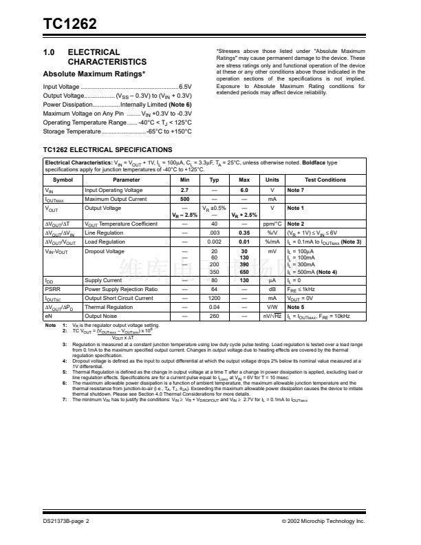
V
OUT
GND
Front View
3
Tab is GND
V
OUT
2
GND
Device Selection Table
Part Number
TC1262-xxVDB
TC1262-xxVAB
TC1262-xxVEB
Package
3-Pin SOT-223
3-Pin TO-220
3-Pin DDPAK
Junction
Temp. Range
-40擄C to +125擄C
-40擄C to +125擄C
-40擄C to +125擄C
TC1262
1
V
IN
General Description
The TC1262 is a fixed output, high accuracy (typically
鹵0.5%) CMOS low dropout regulator. Designed specif-
ically for battery-operated systems, the TC1262鈥檚
CMOS construction eliminates wasted ground current,
significantly extending battery life. Total supply current
is typically 80
碌
A at full load (20 to 60 times lower than
in bipolar regulators).
TC1262 key features include ultra low noise operation,
very low dropout voltage (typically 350mV at full load),
and fast response to step changes in load.
The TC1262 incorporates both over temperature and
over current protection. The TC1262 is stable with an
output capacitor of only 1碌F and has a maximum
output current of 500mA. It is available in 3-Pin
SOT-223, 3-Pin TO-220 and 3-Pin DDPAK packages.
NOTE:
xx indicates output voltages.
Available Output Voltages: 2.5, 2.8, 3.0, 3.3, 5.0.
Other output voltages are available. Please contact Microchip
Technology Inc. for details.
Typical Application
V
IN
V
IN
V
OUT
+
C1
1碌F
V
OUT
TC1262
GND
2002 Microchip Technology Inc.
DS21373B-page 1
V
OUT
V
IN
GND
V
IN
3-Pin SOT-223
漏


 1
1
 2
2
 3
3
 4
4
 5
5
 6
6
 7
7
 8
8
 9
9
 10
10
 11
11
 12
12
