鈥?/div>
Device Marking: Logo, Device Type, e.g., T2500D, Date Code
MAXIMUM RATINGS
(TJ = 25擄C unless otherwise noted)
Rating
Peak Repetitive Off鈥揝tate Voltage(1)
(Sine Wave 50 to 60 Hz, TJ = 鈥?0 to
+100擄C, Gate Open)
On鈥揝tate RMS Current (TC = +80擄C)
(Full Cycle Sine Wave 50 to 60 Hz)
Peak Non鈥搑epetitive Surge Current
(One Full Cycle, 60 Hz, TC = +80擄C)
Circuit Fusing Considerations
(t = 8.3 ms)
Peak Gate Power
(TC = +80擄C, Pulse Width = 10
碌sec)
Average Gate Power
(TC = +80擄C, t = 8.3 ms)
Peak Gate Current
(Pulse Width = 10
碌sec)
Operating Junction Temperature Range
Storage Temperature Range
Symbol
VDRM,
VRRM
IT(RMS)
Value
400
Unit
Volts
4
6.0
A
http://onsemi.com
TRIACS
6 AMPERES RMS
400 VOLTS
MT2
G
MT1
ITSM
I2t
PGM
PG(AV)
IGM
TJ
Tstg
60
15
16
0.2
4.0
鈥?40 to
+125
鈥?40 to
+150
A
A2s
Watts
Watt
1
2
3
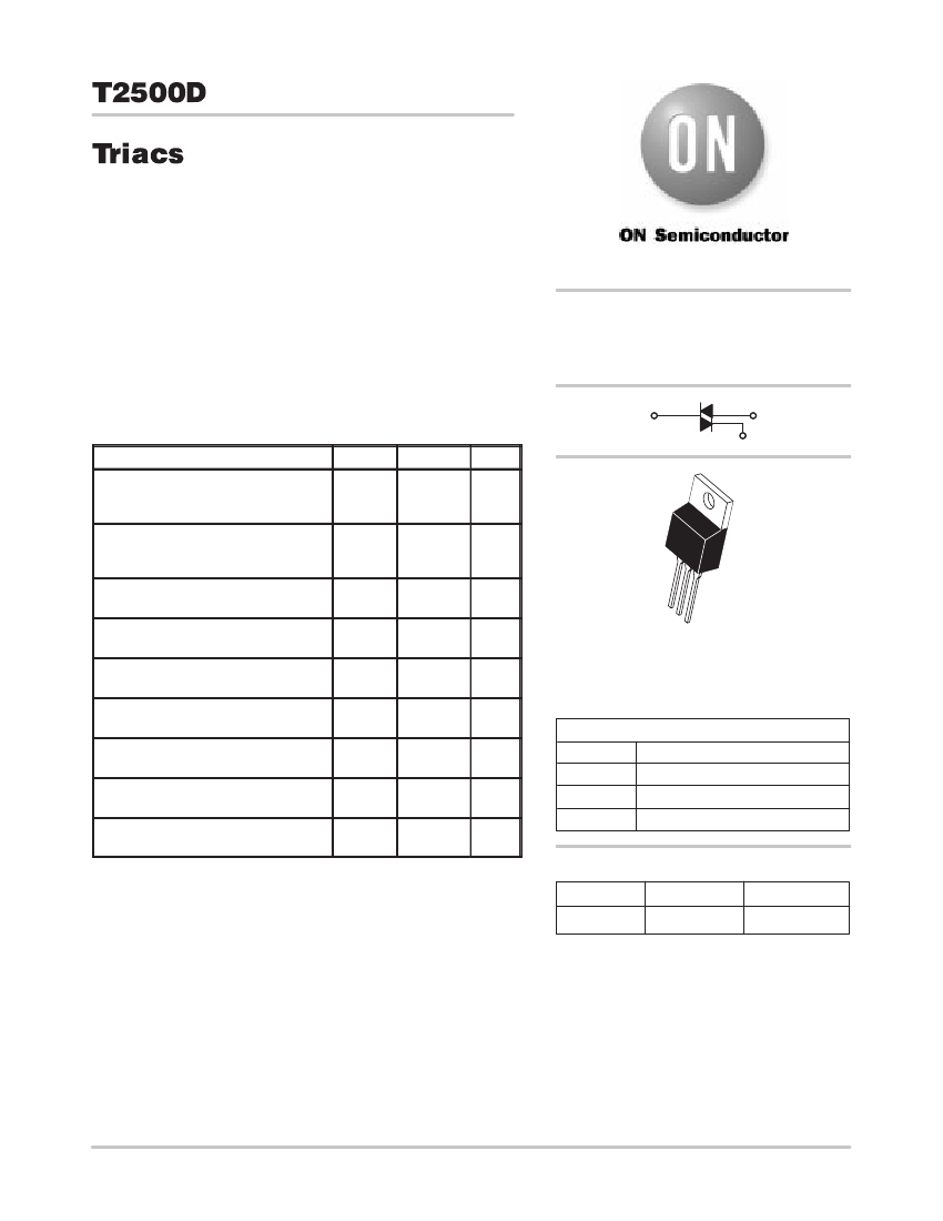
TO鈥?20AB
CASE 221A
STYLE 4
PIN ASSIGNMENT
A
擄C
擄C
1
2
3
4
Main Terminal 1
Main Terminal 2
Gate
Main Terminal 2
(1) VDRM, VRRM for all types can be applied on a continuous basis. Blocking
voltages shall not be tested with a constant current source such that the
voltage ratings of the devices are exceeded.
ORDERING INFORMATION
Device
T2500D
Package
TO220AB
Shipping
500/Box
漏
Semiconductor Components Industries, LLC, 1999
1
February, 2000 鈥?Rev. 2
Publication Order Number:
T2500/D


 1
1
 2
2
 3
3
 4
4
