鈩?/div>
鈥?strip-based process. The resulting
transistor shows extremely high packing density
for low on-resistance, rugged avalanche
characteristics and less critical alignment steps
therefore
a
remarkable
manufacturing
reproducibility.
APPLICATIONS
s
HIGH CURRENT, HIGH SPEED SWITCHING
s
SOLENOID AND RELAY DRIVERS
s
MOTOR CONTROL, AUDIO AMPLIFIERS
s
DC-DC & DC-AC CONVERTERS IN HIGH
PERFORMANCE VRMs
s
AUTOMOTIVE ENVIRONMENT (INJECTION,
ABS, AIR-BAG, LAMPDRIVERS, Etc.)
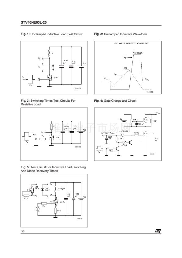
1
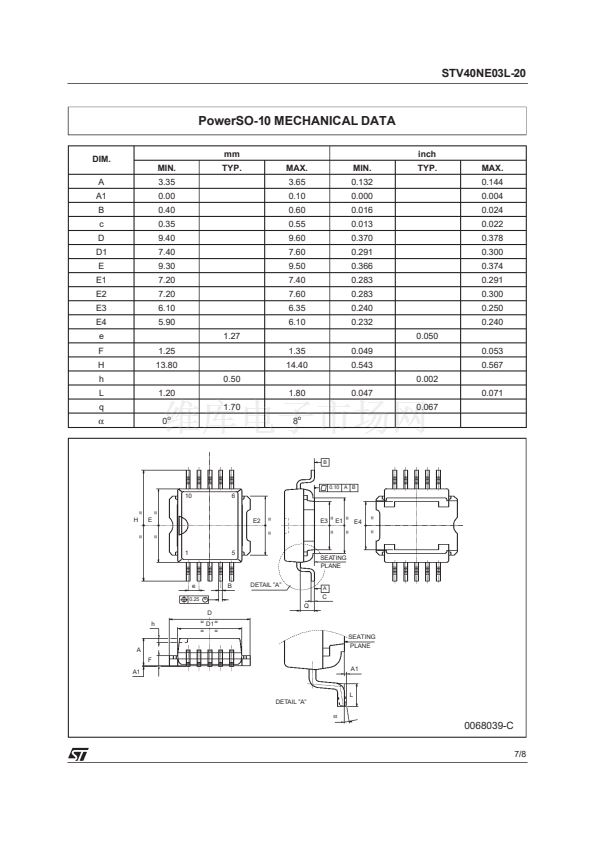
PowerSO-10
INTERNAL SCHEMATIC DIAGRAM
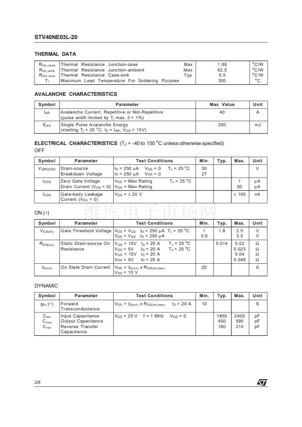
ABSOLUTE MAXIMUM RATINGS
Symb ol
V
DS
V
DGR
V
GS
I
D
I
D
I
DM
(鈥?
P
tot
dv/dt(
1
)
T
st g
T
j
May 2000
Parameter
Drain-source Voltage (V
GS
= 0)
Drain- gate Voltage (R
GS
= 20 k鈩?
Gate-source Voltage
Drain Current (continuous) at T
c
= 25
o
C
Drain Current (continuous) at T
c
= 100 C
Drain Current (pulsed)
Total Dissipation at T
c
= 25
o
C
Derating F actor
Peak Diode Recovery voltage slope
Storage T emperature
Max. Operating Junction Temperature
o
Value
30
30
鹵
20
40
28
160
80
0.53
7
-65 to 175
175
(
1
) I
SD
鈮?/div>
40 A, di/dt
鈮?/div>
300 A/碌s, V
DD
鈮?/div>
V
(BR)DSS
, T
j
鈮?/div>
T
JMAX
Unit
V
V
V
A
A
A
W
W /
o
C
V/ns
o
o
C
C
1/8
(鈥? Pulse width limited by safe operating area


 1
1
 2
2
 3
3
 4
4
 5
5
 6
6
 7
7
 8
8
