STMicroelectronics well established STripFET鈩?/div>
process based on a very unique strip layout
design. The resulting MOSFET shows unrivalled
high packing density with ultra low on-resistance
and superior switching charactestics. Process
simplification also translates into improved
manufacturing reproducibility. This device is
particularly suitable for high current, low voltage
switching application where efficiency is crucial.
APPLICATIONS
s
BUCK CONVERTERS IN HIGH
PERFORMACE TELECOM AND VRMs
DC-DC CONVERTERS
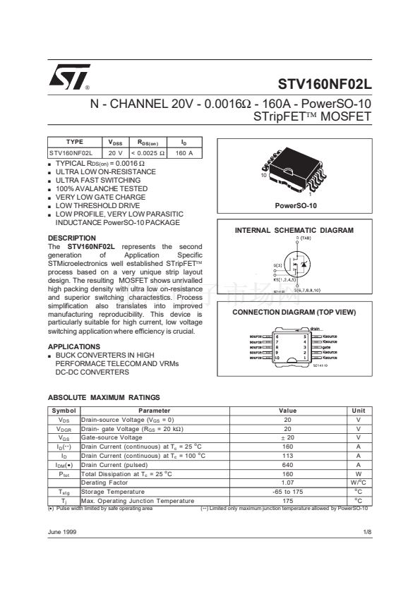
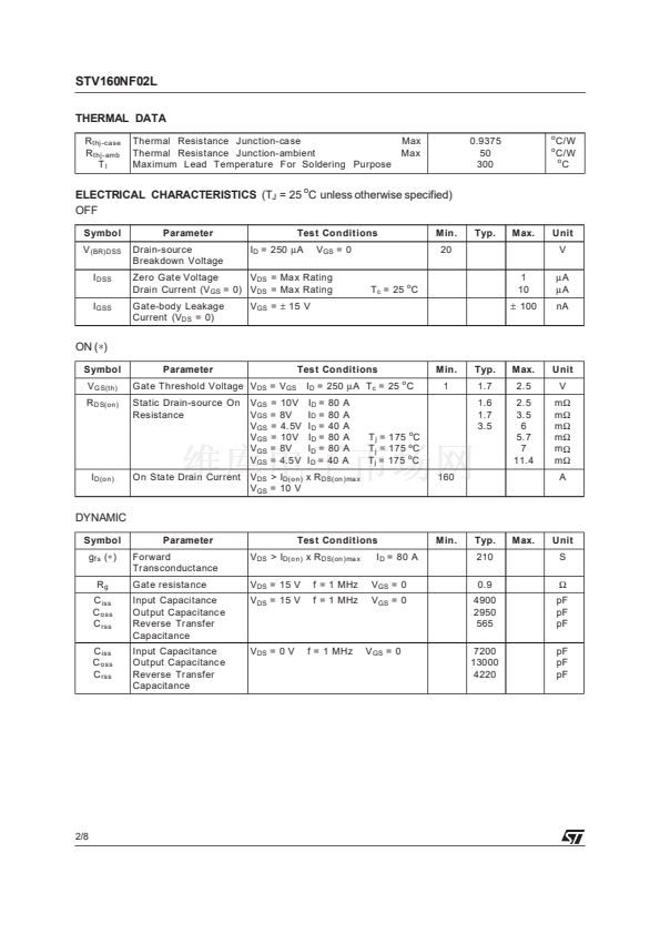
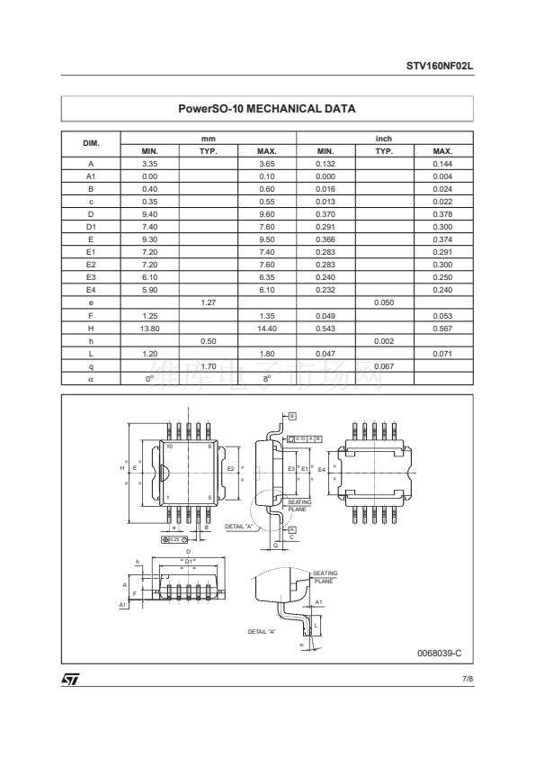
CONNECTION DIAGRAM (TOP VIEW)
ABSOLUTE MAXIMUM RATINGS
Symb ol
V
DS
V
DGR
V
GS
I
D
(
* *
)
I
D
I
DM
(
鈥?/div>
)
P
tot
T
st g
T
j
Parameter
Drain-source Voltage (V
GS
= 0)
Drain- gate Voltage (R
GS
= 20 k鈩?
Gate-source Voltage
Drain Current (continuous) at T
c
= 25 C
Drain Current (continuous) at T
c
= 100
o
C
Drain Current (pulsed)
T otal Dissipation at T
c
= 25
o
C
Derating F actor
Storage Temperature
Max. Operating Junction T emperature
o
Value
20
20
鹵
20
160
113
640
160
1.07
-65 to 175
175
Unit
V
V
V
A
A
A
W
W /
o
C
o
C
o
C
(鈥? Pulse width limited by safe operating area
(
**
) Limited only maximum junction temperature allowed by PowerSO-10
June 1999
1/8


 1
1
 2
2
 3
3
 4
4
 5
5
 6
6
 7
7
 8
8
