ity in off-line quasi-resonant flyback converters. These devices incorpo-
generation high-voltage bipolar switching transistor.
28113鈥?/div>
BASE
3
SINK
4
OSC.
R
DRIVE
OVER-CURRENT
PROTECTION
FDBK
5
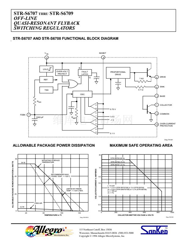
Crucial system parameters such as maximum ON time and OFF
time are fixed during manufacture. Local control circuit decoupling and
layout are optimized within each device.
Cycle-by-cycle current limiting, under-voltage lock-out with hyster-
esis, over-voltage protection, and thermal shutdown protect these
devices during all normal and overload conditions. Over-voltage
protection and thermal shutdown are latched after a short delay. A
versatile triple-level inhibit circuit includes the OFF time synchronization
required to establish quasi-resonant operation. The inhibit function has
also been expanded to initiate operation in stand-by mode in which the
power supply delivers a small fraction of the steady-state output power.
The dual requirements of dielectric isolation and low transient thermal
impedance and steady-state thermal resistance are satisfied in an over-
molded single-in-line power package.
6
+
REF.
7
INHIBIT
8
UVLO
V IN
9
Dwg. PK-001
ABSOLUTE MAXIMUM RATINGS
Supply Voltage, V
IN
...........................
15 V
Output Voltage, V
CEX
.......................
850 V
V
EBO
................................................
7 V
Continuous Output Current,
I
C
..........................................
See Table
1 ms Single-Pulse Output Current,
I
CM
........................................
See Table
Sink Current, I
S
.........................
See Table
Drive Current, I
D
..........................
-700 mA
Feedback Current, I
FDBK
.................
20 mA
Inhibit Voltage, V
INH
...........................
15 V
Over-Current Protection Voltage Range,
V
OCP
............................................
鹵
3.5 V
Insulation Voltage,V
WM(RMS)
...........
2000 V
Package Power Diss., P
D
........
See Graph
Output Junction Temperature, T
J
..
+150
擄
C
Internal Frame Temperature, T
F
...
+125
擄
C
Operating Temperature Range,
T
A
...............................
-20
擄
C to +125
擄
C
Storage Temperature Range,
T
stg
.............................
-40
擄
C to +125
擄
C
I
D
C
S
N
O
F
I
T
U
N
Proven in substantial volumes, these devices and their fixed-
frequency counterparts represent a significant advance in off-line SMPS
reliability growth and integration.
D
E
P
FEATURES
R
O
R
s
Quasi-Resonant Operation for Low EMI and High Efficiency
s
Output Power to 220 W
s
Low-Power Output Standby Mode
s
Pulse-by-Pulse Over-Current Protection
s
Latched Over-Voltage and Thermal Protection
s
Third-Generation Switching Transistor with Proportional Drive
s
Maximum ON Time and Off Time Set During Manufacture
s
Internal Under-Voltage Lockout with Hysteresis
s
Over-Molded SIP with Integral Isolated Heat Spreader
F
E
R
E
E
C
N
E
O
R
T
C
U
Y
D
L
N
O
鈥?/div>
+
Always order by complete part number:
Max. Cont.
Peak
Part Number
Current, I
C
Current, I
CM
STR-S6707
STR-S6708
STR-S6709
6A
7.5 A
10 A
12 A
15 A
20 A
Max. Sink
Current, I
S
1.5 A
1.5 A
2A
鈩?/div>
next


 1
1
 2
2
 3
3
 4
4
 5
5
 6
6
 7
7
 8
8
