鈩?/div>
EXCEPTIONAL dv/dt CAPABILITY
AVALANCHE RUGGED TECHNOLOGY
100 % AVALANCHE TESTED
APPLICATION ORIENTED
CHARACTERIZATION
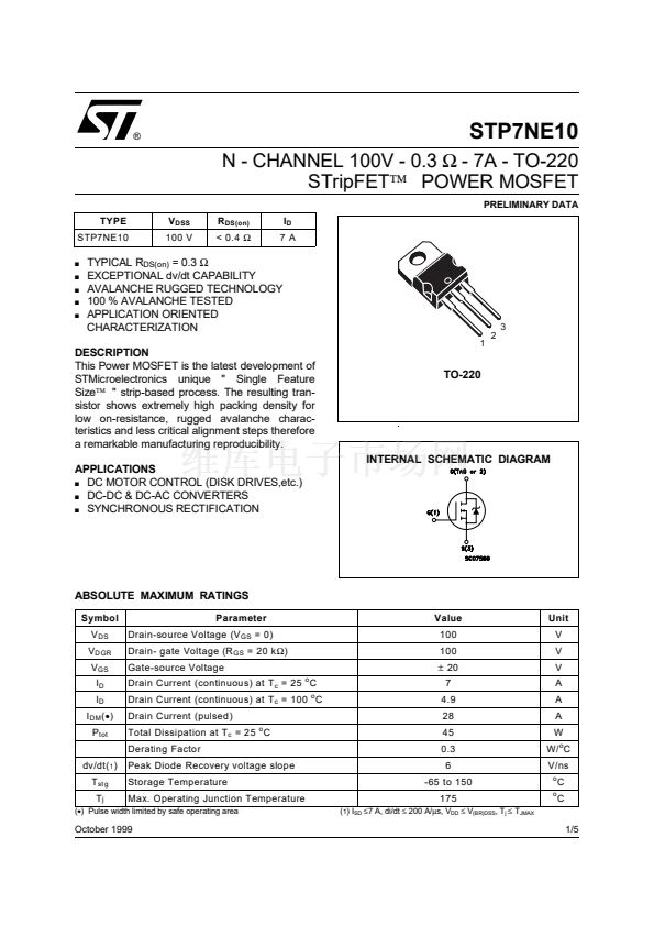
1
3
2
DESCRIPTION
This Power MOSFET is the latest development of
STMicroelectronics unique " Single Feature
Size鈩?" strip-based process. The resulting tran-
sistor shows extremely high packing density for
low on-resistance, rugged avalanche charac-
teristics and less critical alignment steps therefore
a remarkable manufacturing reproducibility.
APPLICATIONS
s
DC MOTOR CONTROL (DISK DRIVES,etc.)
s
DC-DC & DC-AC CONVERTERS
s
SYNCHRONOUS RECTIFICATION
TO-220
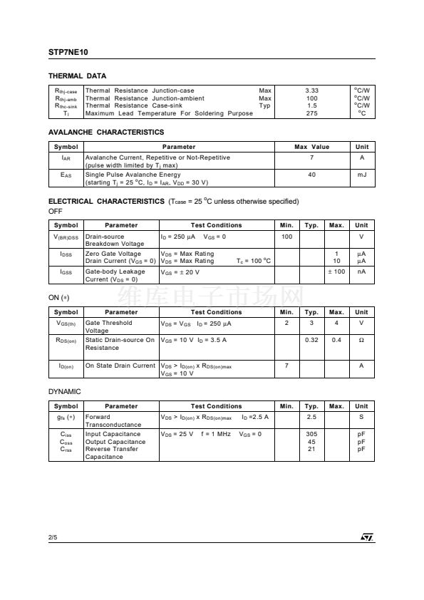
INTERNAL SCHEMATIC DIAGRAM
ABSOLUTE MAXIMUM RATINGS
Symbol
V
DS
V
DGR
V
GS
I
D
I
D
I
DM
(鈥?
P
tot
dv/dt(
1
)
T
st g
T
j
Parameter
Drain-source Voltage (V
GS
= 0)
Drain- gate Voltage (R
GS
= 20 k鈩?
Gate-source Voltage
Drain Current (continuous) at T
c
= 25
o
C
Drain Current (continuous) at T
c
= 100
o
C
Drain Current (pulsed)
Total Dissipation at T
c
= 25 C
Derating Factor
Peak Diode Recovery voltage slope
Storage Temperature
Max. Operating Junction Temperature
o
Value
100
100
鹵
20
7
4.9
28
45
0.3
6
-65 to 150
175
(
1
) I
SD
鈮?
A, di/dt
鈮?/div>
200 A/碌s, V
DD
鈮?/div>
V
(BR)DSS
, T
j
鈮?/div>
T
JMAX
Unit
V
V
V
A
A
A
W
W/
o
C
V/ns
o
o
C
C
1/5
(鈥? Pulse width limited by safe operating area
October 1999


 1
1
 2
2
 3
3
 4
4
 5
5
