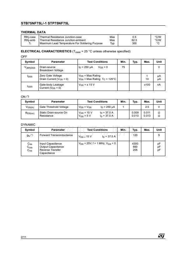
(on) = 0.009鈩?/div>
EXCEPTIONAL dv/dt CAPABILITY
100% AVALANCHE TESTED
LOW THRESHOLD DRIVE
3
12
D
2
PAK
TO-263
I
2
PAK
TO-262
DESCRIPTION
This MOSFET series realized with STMicroelectronics
unique STripFET process has specifically been designed
to minimize input capacitance and gate charge. It is
therefore suitable as primary switch in advanced high-
efficiency, high-frequency isolated DC-DC converters for
Telecom and Computer applications. It is also intended
for any applications with low gate drive requirements
.
3
1
2
TO-220
INTERNAL SCHEMATIC DIAGRAM
APPLICATIONS
s
SOLENOID AND RELAY DRIVERS
s
DC MOTOR CONTROL
s
DC-DC CONVERTERS
s
AUTOMOTIVE ENVIRONMENT
ABSOLUTE MAXIMUM RATINGS
Symbol
V
DS
V
DGR
V
GS
I
D
(鈥?
I
D
I
DM
(鈥⑩€?
P
tot
dv/dt
(1)
E
AS (2)
T
stg
T
j
Parameter
Drain-source Voltage (V
GS
= 0)
Drain-gate Voltage (R
GS
= 20 k鈩?
Gate- source Voltage
Drain Current (continuous) at T
C
= 25擄C
Drain Current (continuous) at T
C
= 100擄C
Drain Current (pulsed)
Total Dissipation at T
C
= 25擄C
Derating Factor
Peak Diode Recovery voltage slope
Single Pulse Avalanche Energy
Storage Temperature
Max. Operating Junction Temperature
Value
75
75
鹵 15
75
70
300
300
2
20
680
-55 to 175
Unit
V
V
V
A
A
A
W
W/擄C
V/ns
mJ
擄C
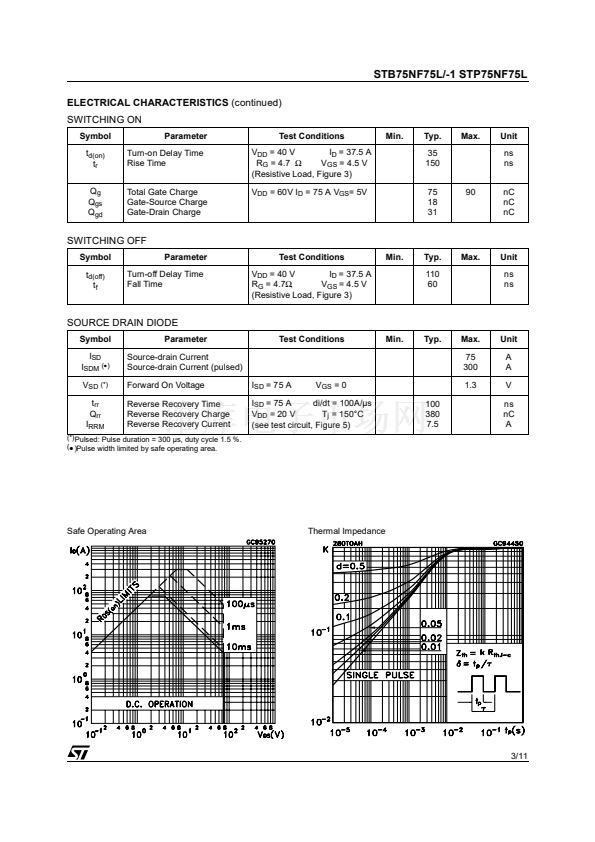
(鈥? Current limited by package
(鈥⑩€?
Pulse width limited by safe operating area.
April 2002
.
(1) I
SD
鈮?/div>
75A, di/dt
鈮?/div>
500A/碌s, V
DD
鈮?/div>
V
(BR)DSS
, T
j
鈮?/div>
T
JMAX.
(2) Starting T
j
= 25
o
C, I
D
= 37.5A, V
DD
= 30V
1/11


 1
1
 2
2
 3
3
 4
4
 5
5
 6
6
 7
7
 8
8
 9
9
 10
10
 11
11
