鈩?/div>
100% AVALANCHE TESTED
LOW CAPACITANCE AND GATE CHARGE
175
o
C MAXIMUM JUNCTION
TEMPERATURE
3
1
2
DESCRIPTION
This fully clamped Mosfet is produced by using
the latest advanced Company鈥檚 Mesh Overlay
process which is based on a novel strip layout.
The inherent benefits of the new technology
coupled with the extra clamping capabilities make
this product particularly suitable for the harshest
operation conditions such as those encountered
in the automotive environment. Any other
application requiring extra ruggedness is also
recommended.
APPLICATIONS
s
ABS, SOLENOID DRIVERS
s
MOTOR CONTROL
s
DC-DC CONVERTERS
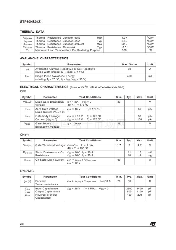
ABSOLUTE MAXIMUM RATINGS
Symbol
V
DS
V
DG
V
GS
I
D
I
D
I
DG
I
GS
I
DM
(鈥?
P
tot
Drain- gate Voltage
G ate-source Voltage
Drain Current (continuous) at T
c
= 25
o
C
Drain Current (continuous) at T
c
= 100 C
Drain Gate Current (continuous)
G ate Source Current (continuous)
Drain Current (pulsed)
T otal Dissipation at T
c
= 25 C
Derating Factor
V
ESD
(G-S )
G ate-Source ESD (HBM - C= 100pF , R=1.5 k
鈩?/div>
)
V
ESD
(G-D)
G ate-Drain ESD (HBM - C= 100pF, R=1.5 k鈩?
V
ESD
( D-S)
Drain-Source ESD (HBM - C= 100pF, R=1.5 k鈩?
T
s tg
T
j
Storage Temperature
Max. Operating Junction Temperature
o
o
TO-220
INTERNAL SCHEMATIC DIAGRAM
Parameter
Drain-source Voltage (V
GS
= 0)
Value
CLAMPED
CLAMPED
CLAMPED
60
42
鹵
50
鹵
50
240
140
0.93
2
4
4
-65 to 175
-40 to 175
(
1
) I
SD
鈮?0
A, di/dt
鈮?/div>
300 A/碌s, V
DD
鈮?/div>
V
(BR)DSS
, T
j
鈮?/div>
T
JMAX
Un it
V
V
V
A
A
mA
mA
A
W
W /
o
C
kV
kV
kV
o
o
C
C
1/8
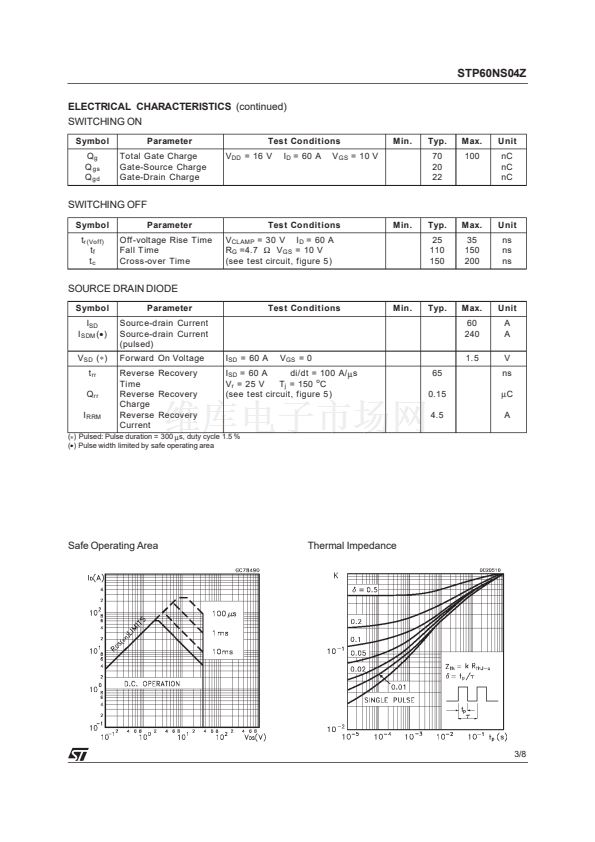
(鈥? Pulse width limited by safe operating area
December 1999


 1
1
 2
2
 3
3
 4
4
 5
5
 6
6
 7
7
 8
8
