鈩?/div>
100% AVALANCHE TESTED
LOW CAPACITANCE AND GATE CHARGE
175擄C MAXIMUM JUNCTION TEMPERATURE
1
3
2
DESCRIPTION
This fully clamped MOSFET is produced by using
the latest advanced Company鈥檚 Mesh Overlay pro-
cess which is based on a novel strip layout. The in-
herent benefits of the new technology coupled with
the extra clamping capabilities make this product
particularly suitable for the harshest operation con-
ditions such as those encountered in the automotive
environment .Any other application requiring extra
ruggedness is also recommended.
APPLICATIONS
s
ABS,SOLENOID DRIVERS
s
MOTOR CONTROL
s
DC-DC CONVERTERS
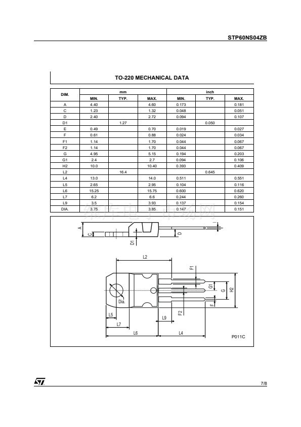
TO-220
INTERNAL SCHEMATIC DIAGRAM
ABSOLUTE MAXIMUM RATINGS
Symbol
V
DS
V
DG
V
GS
I
D
I
D
I
DG
I
GS
I
DM
( )
P
TOT
V
ESD(G-S)
V
ESD(G-D)
V
ESD(D-S)
T
stg
T
j
Parameter
Drain-source Voltage (V
GS
= 0)
Drain-gate Voltage
Gate- source Voltage
Drain Current (continuous) at T
C
= 25擄C
Drain Current (continuous) at T
C
= 100擄C
Drain Gate Current (continuous)
Gate Source Current (continuous)
Drain Current (pulsed)
Total Dissipation at T
C
= 25擄C
Derating Factor
Gate-Source ESD(HBM-C=100 pF, R=1.5 K鈩?
Gate-Drain ESD(HBM-C=100 pF, R=1.5 K鈩?
Drain-Source ESD(HBM-C=100 pF, R=1.5 K鈩?
Storage Temperature
Max. Operating Junction Temperature
Value
CLAMPED
CLAMPED
CLAMPED
60
42
鹵
50
鹵
50
240
150
1
6
4
4
鈥?5 to 175
Unit
V
V
V
A
A
mA
mA
A
W
W/擄C
kV
kV
kV
擄C
(鈥?Pulse width limited by safe operating area
November 2002
1/8


 1
1
 2
2
 3
3
 4
4
 5
5
 6
6
 7
7
 8
8
