Using the latest high voltage MESH OVERLAY鈩?/div>
process, STMicroelectronics has designed an advanced
family
of
power
MOSFETs
with
outstanding
performances. The new patent pending strip layout
coupled with the Company鈥檚 proprietary edge termination
structure, gives the lowest RDS(on) per area,
exceptional avalanche and dv/dt capabilities and
unrivalled gate charge and switching characteristics.
3
1
2
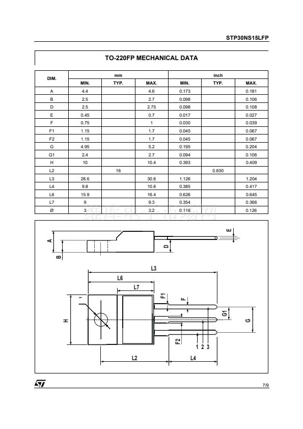
TO-220FP
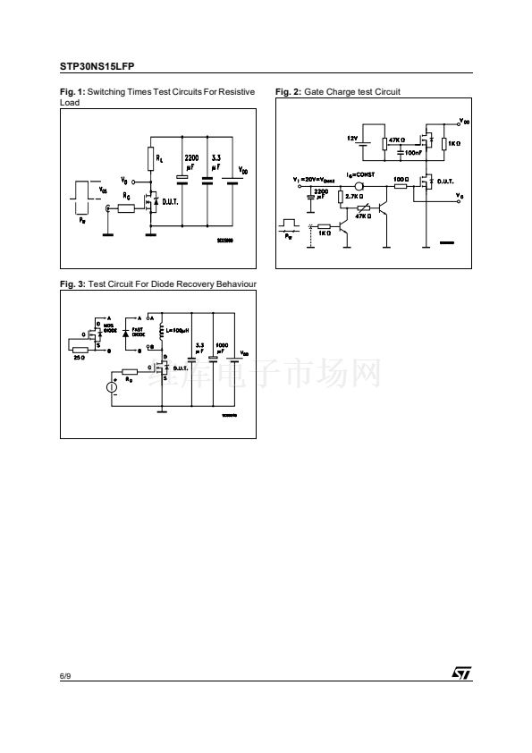
INTERNAL SCHEMATIC DIAGRAM
APPLICATIONS
s
SWITCHING 鈥淪鈥?CAPACITOR
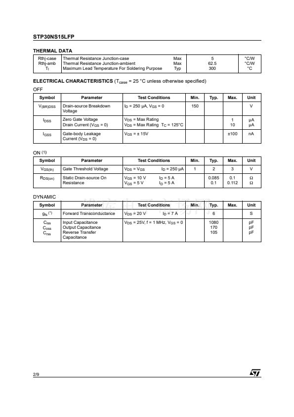
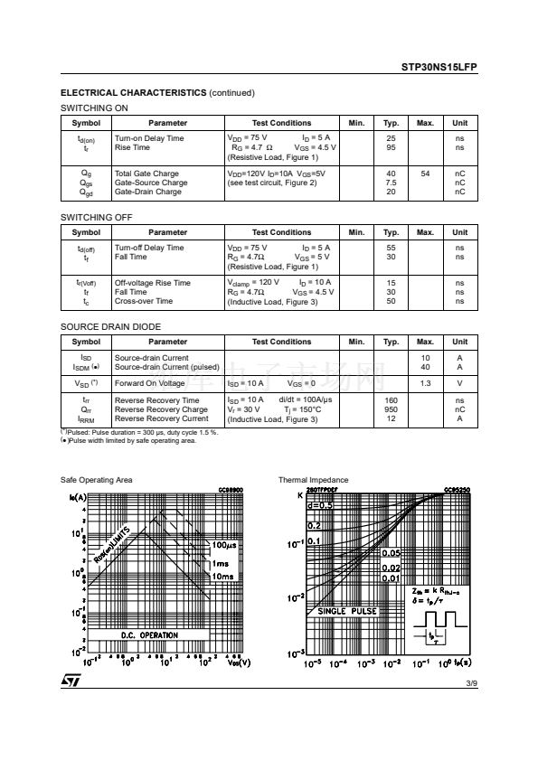
ABSOLUTE MAXIMUM RATINGS
Symbol
V
DS
V
DGR
V
GS
I
D
I
D
I
DM
(鈥?
P
tot
E
AS
(1)
dv/dt
(2)
T
stg
T
j
Parameter
Drain-source Voltage (V
GS
= 0)
Drain-gate Voltage (R
GS
= 20 k鈩?
Gate- source Voltage
Drain Current (continuous) at T
C
= 25擄C
Drain Current (continuous) at T
C
= 100擄C
Drain Current (pulsed)
Total Dissipation at T
C
= 25擄C
Derating Factor
Single Pulse Avalanche Energy
Peak Diode Recovery voltage slope
Storage Temperature
Operating Junction Temperature
Value
150
150
鹵 15
10
7
40
30
0.2
300
2.4
-55 to 175
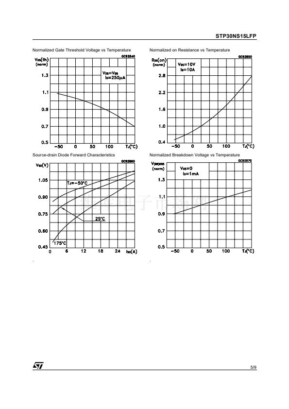
(1) Starting T
j
= 25
o
C, I
D
= 15A, V
DD
= 75V
(2) I
SD
鈮?5A,
di/dt
鈮?00A/碌s,
V
DD
鈮?/div>
V
(BR)DSS
, T
j
鈮?/div>
T
JMAX.
Unit
V
V
V
A
A
A
W
W/擄C
mJ
V/ns
擄C
(鈥?
Pulse width limited by safe operating area.
July 2003
.
1/9


 1
1
 2
2
 3
3
 4
4
 5
5
 6
6
 7
7
 8
8
 9
9
