(on) = 0.007鈩?/div>
EXCEPTIONAL dv/dt CAPABILITY
100% AVALANCHE TESTED
SURFACE-MOUNTING D
2
PAK (TO-263)
POWER PACKAGE IN TUBE (NO SUFFIX) OR
IN TAPE & REEL (SUFFIX 鈥淭4鈥?
3
1
3
1
2
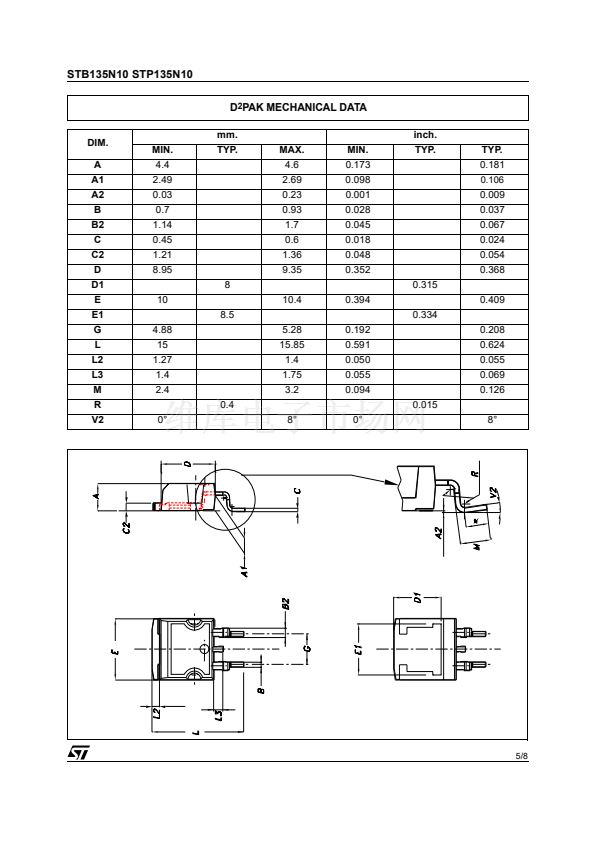
D
2
PAK
TO-263
(Suffix 鈥淭4鈥?
TO-220
DESCRIPTION
This MOSFET is the result of STMicroelectronics鈥檚 well
established and consolidated STripFET technology utiliz-
ing the most recent layout optimization. The device exhib-
its extremely low on-resistance, gate charge and diode鈥檚
reverse recovery charge Qrr making it the ideal switch in
a very large spectrum of applications such as Automotive,
Consumer, Telecom and Industrial.
INTERNAL SCHEMATIC DIAGRAM
APPLICATIONS
s
PRIMARY SWITCH IN TELECOM DC-DC
CONVERTER
s
HIGH-EFFICIENCY DC-DC CONVERTERS
s
42V AUTOMOTIVE APPLICATIONS
s
SYNCHRONOUS RECTIFICATION
s
DIESEL INJECTION
s
PWM UPS AND MOTOR CONTROL
ABSOLUTE MAXIMUM RATINGS
Symbol
V
DS
V
DGR
V
GS
I
D(*)
I
D
I
DM(1)
P
tot
dv/dt
(2)
E
AS (3)
T
stg
T
j
Parameter
Drain-source Voltage (V
GS
= 0)
Drain-gate Voltage (R
GS
= 20 k鈩?
Gate- source Voltage
Drain Current (continuous) at T
C
= 25擄C
Drain Current (continuous) at T
C
= 100擄C
Drain Current (pulsed)
Total Dissipation at T
C
= 25擄C
Derating Factor
Peak Diode Recovery voltage slope
Single Pulse Avalanche Energy
Storage Temperature
Operating Junction Temperature
Value
100
100
鹵 20
135
96
540
150
1
TBD
TBD
-55 to 175
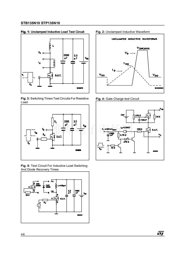
(2) I
SD
鈮?/div>
40A, di/dt
鈮?/div>
600A/碌s, V
DD
鈮
VDSS
, T
j
鈮?/div>
T
JMAX.
(3) Starting T
j
= 25
o
C, I
D
= 40A, V
DD
= 50V
Unit
V
V
V
A
A
A
W
W/擄C
V/ns
mJ
擄C
(1)
Pulse width limited by safe operating area.
(*)
Value limited by wire bonding
July 2003
This is preliminary information on a new product forseen to be developped. Details are subject to change without notice
1/8


 1
1
 2
2
 3
3
 4
4
 5
5
 6
6
 7
7
 8
8
