鈩?/div>
APPLICATION ORIENTED
CHARACTERIZATION
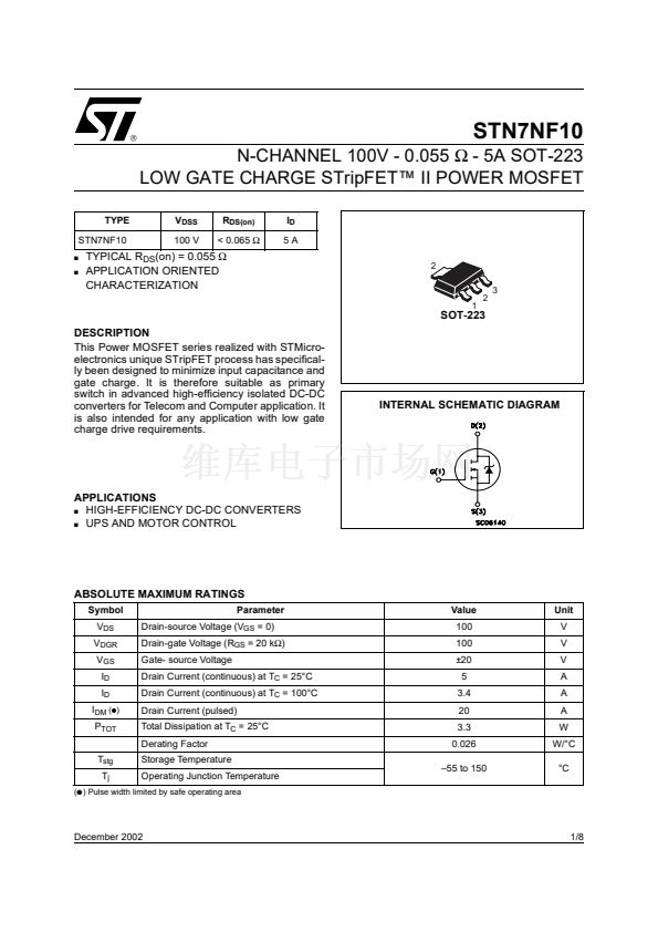
1
2
3
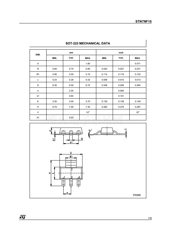
SOT-223
DESCRIPTION
This Power MOSFET series realized with STMicro-
electronics unique STripFET process has specifical-
ly been designed to minimize input capacitance and
gate charge. It is therefore suitable as primary
switch in advanced high-efficiency isolated DC-DC
converters for Telecom and Computer application. It
is also intended for any application with low gate
charge drive requirements.
INTERNAL SCHEMATIC DIAGRAM
APPLICATIONS
s
HIGH-EFFICIENCY DC-DC CONVERTERS
s
UPS AND MOTOR CONTROL
ABSOLUTE MAXIMUM RATINGS
Symbol
V
DS
V
DGR
V
GS
I
D
I
D
I
DM
( )
P
TOT
T
stg
T
j
Parameter
Drain-source Voltage (V
GS
= 0)
Drain-gate Voltage (R
GS
= 20 k鈩?
Gate- source Voltage
Drain Current (continuous) at T
C
= 25擄C
Drain Current (continuous) at T
C
= 100擄C
Drain Current (pulsed)
Total Dissipation at T
C
= 25擄C
Derating Factor
Storage Temperature
Operating Junction Temperature
Value
100
100
鹵20
5
3.4
20
3.3
0.026
鈥?5 to 150
Unit
V
V
V
A
A
A
W
W/擄C
擄C
(
q
) Pulse width limited by safe operating area
December 2002
1/8


 1
1
 2
2
 3
3
 4
4
 5
5
 6
6
 7
7
 8
8
