鈩?/div>
@ 4.5 V
R
DS(ON)
* Qg INDUSTRY鈥檚 BENCHMARK
CONDUCTION LOSSES REDUCED
SWITCHING LOSSES REDUCED
LOW THRESHOLD DEVICE
THROUGH-HOLE IPAK (TO-251) POWER
PACKAGE IN TUBE (SUFFIX 鈥?1")
SURFACE-MOUNTING DPAK (TO-252)
POWER PACKAGE IN TAPE & REEL
(SUFFIX 鈥淭4")
3
2
1
IPAK
TO-251
(Suffix 鈥?1鈥?
DPAK
TO-252
(Suffix 鈥淭4鈥?
3
1
INTERNAL SCHEMATIC DIAGRAM
DESCRIPTION
The STD55NH2LL is based on the latest generation of
ST's proprietary STripFET鈩?technology. An innovative
layout enables the device to also exhibit extremely low
gate charge for the most demanding requirements as
high-side switch in high-frequency DC-DC converters. It's
therefore ideal for high-density converters in Telecom
and Computer applications.
APPLICATIONS
s
SPECIFICALLY DESIGNED AND OPTIMISED
FOR HIGH EFFICIENCY DC/DC CONVERTES
Ordering Information
SALES TYPE
STD55NH2LLT4
STD55NH2LL-1
MARKING
D55NH2LL
D55NH2LL
PACKAGE
TO-252
TO-251
PACKAGING
TAPE & REEL
TUBE
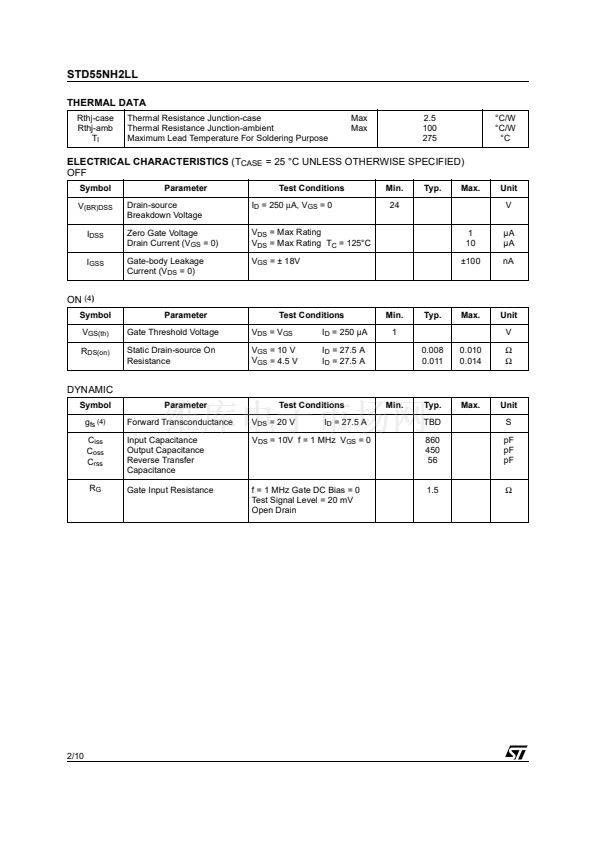
ABSOLUTE MAXIMUM RATINGS
Symbol
V
spike(1)
V
DS
V
DGR
V
GS
I
D
I
D
I
DM(2)
P
tot
E
AS(3)
T
stg
T
j
Parameter
Drain-source Voltage Rating
Drain-source Voltage (V
GS
= 0)
Drain-gate Voltage (R
GS
= 20 k鈩?
Gate- source Voltage
Drain Current (continuous) at T
C
= 25擄C
Drain Current (continuous) at T
C
= 100擄C
Drain Current (pulsed)
Total Dissipation at T
C
= 25擄C
Derating Factor
Single Pulse Avalanche Energy
Storage Temperature
Operating Junction Temperature
Value
30
24
24
鹵 18
55
39
220
60
0.4
TBD
-55 to 175
Unit
V
V
V
V
A
A
A
W
W/擄C
mJ
擄C
1/10
September 2003
This is preliminary information on a new product forseen to be developped. Details are subject to change without notice


 1
1
 2
2
 3
3
 4
4
 5
5
 6
6
 7
7
 8
8
 9
9
 10
10
