鈩?/div>
鈥?strip-based process. The resul-
ting transistor shows the best trade-off between
on-resistance and gate charge. When used as
high and low side in buck regulators, it gives the
best performance in terms of both conduction and
switching losses. This is extremely important for
motherboards where fast switching and high effi-
ciency are of paramount importance.
APPLICATIONS
s
SPECIFICALLY DESIGNED AND
OPTIMISED FOR HIGH EFFICIENCY CPU
CORE DC/DC CONVERTERS
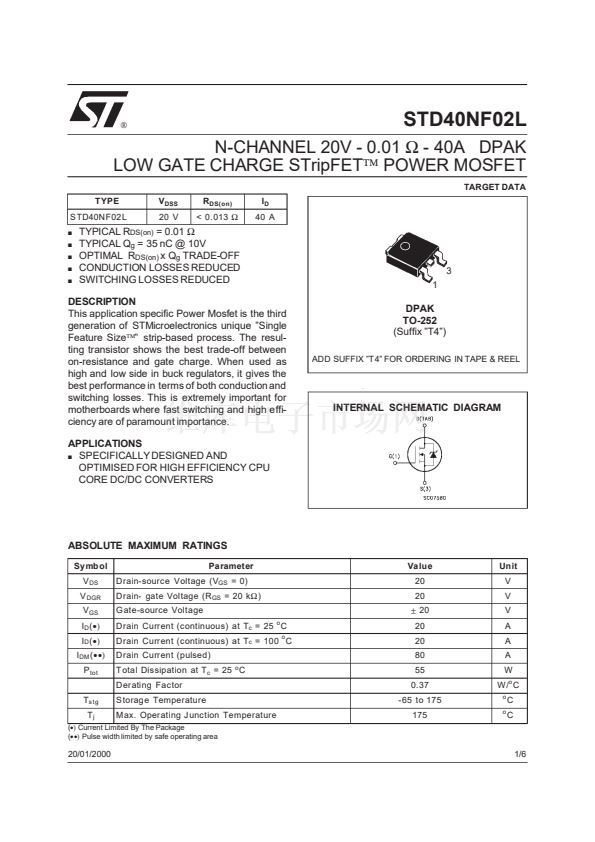
DPAK
TO-252
(Suffix 鈥漈4鈥?
ADD SUFFIX 鈥漈4鈥?FOR ORDERING IN TAPE & REEL
INTERNAL SCHEMATIC DIAGRAM
ABSOLUTE MAXIMUM RATINGS
Symbol
V
DS
V
DGR
V
GS
I
D
(鈥?
I
D
(鈥?
I
DM
(鈥⑩€?
P
tot
T
s tg
T
j
Parameter
Drain-source Voltage (V
GS
= 0)
Drain- gate Voltage (R
GS
= 20 k鈩?
G ate-source Voltage
Drain Current (continuous) at T
c
= 25
o
C
Drain Current (continuous) at T
c
= 100 C
Drain Current (pulsed)
T otal Dissipation at T
c
= 25
o
C
Derating Factor
Storage Temperature
Max. Operating Junction Temperature
o
Value
20
20
鹵
20
20
20
80
55
0.37
-65 to 175
175
Un it
V
V
V
A
A
A
W
W /
o
C
o
o
C
C
(鈥? Current Limited By The Package
(鈥⑩€? Pulse width limited by safe operating area
20/01/2000
1/6


 1
1
 2
2
 3
3
 4
4
 5
5
 6
6
