Using the latest high voltage MESH OVERLAY鈩?/div>
process, STMicroelectronics has designed an ad-
vanced family of power MOSFETs with outstanding
performances. The new patent pending strip layout
coupled with the Company鈥檚 proprieraty edge termi-
nation structure, gives the lowest RDS(on) per area,
exceptional avalanche and dv/dt capabilities and
unrivalled gate charge and switching characteris-
tics.
APPLICATIONS
s
SWITH MODE POWER SUPPLIES (SMPS)
s
LIGHTING FOR INDUSTRIAL AND CONSUMER
ENVIRONMENT
INTERNAL SCHEMATIC DIAGRAM
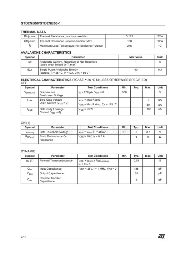
ABSOLUTE MAXIMUM RATINGS
Symbol
V
DS
V
DGR
V
GS
I
D
I
D
I
DM
(
q
)
P
TOT
dv/dt(1)
T
stg
T
j
Parameter
Drain-source Voltage (V
GS
= 0)
Drain-gate Voltage (R
GS
= 20 k鈩?
Gate- source Voltage
Drain Current (continuos) at T
C
= 25擄C
Drain Current (continuos) at T
C
= 100擄C
Drain Current (pulsed)
Total Dissipation at T
C
= 25擄C
Derating Factor
Peak Diode Recovery voltage slope
Storage Temperature
Max. Operating Junction Temperature
Value
500
500
鹵
30
1
0.63
4
40
0.32
3.5
鈥?5 to 150
150
(1)I
SD
鈮?A,
di/dt
鈮?00A/碌s,
V
DD
鈮?/div>
V
(BR)DSS
, T
j
鈮?/div>
T
JMAX.
Unit
V
V
V
A
A
A
W
W/擄C
V/ns
擄C
擄C
1/10
(鈥?Pulse width limited by safe operating area
September 2001


 1
1
 2
2
 3
3
 4
4
 5
5
 6
6
 7
7
 8
8
 9
9
 10
10
