鈩⑩€?/div>
strip-based process. The resulting
transistor shows the best trade-off between on-re-
sistance and gate charge. When used as high and
low side in buck regulators, it gives the best perfor-
mance in terms of both conduction and switching
losses. This is extremely important for mother-
boards where fast switching and high efficiency are
of paramount importance.
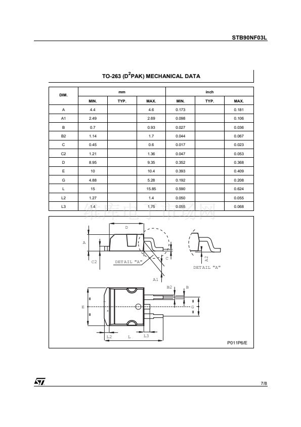
D
2
PAK
INTERNAL SCHEMATIC DIAGRAM
s
APPLICATIONS
SPECIFICALLY DESIGNED AND OPTIMISED
FOR HIGH EFFICIENCY CPU CORE DC/DC
CONVERTERS
ABSOLUTE MAXIMUM RATINGS
Symbol
V
DS
V
DGR
V
GS
I
D
I
D
I
DM
(
q
)
P
TOT
T
stg
T
j
Parameter
Drain-source Voltage (V
GS
= 0)
Drain-gate Voltage (R
GS
= 20 k鈩?
Gate- source Voltage
Drain Current (continuos) at T
C
= 25擄C
Drain Current (continuos) at T
C
= 100擄C
Drain Current (pulsed)
Total Dissipation at T
C
= 25擄C
Derating Factor
Storage Temperature
Max. Operating Junction Temperature
Value
30
30
鹵 18
90
65
360
150
0.73
鈥?55 to 175
Unit
V
V
V
A
A
A
W
W/擄C
擄C
(
q
) Pulse width limited by safe operating area
October 2001
1/8


 1
1
 2
2
 3
3
 4
4
 5
5
 6
6
 7
7
 8
8
