鈩?/div>
EXTREMELY HIGH dv/dt CAPABILITY
100% AVALANCHE TESTED
VERY LOW INTRINSIC CAPACITANCES
GATE CHARGE MINIMIZED
FOR THROUGH-HOLE VERSION CONTACT
SALES OFFICE
3
1
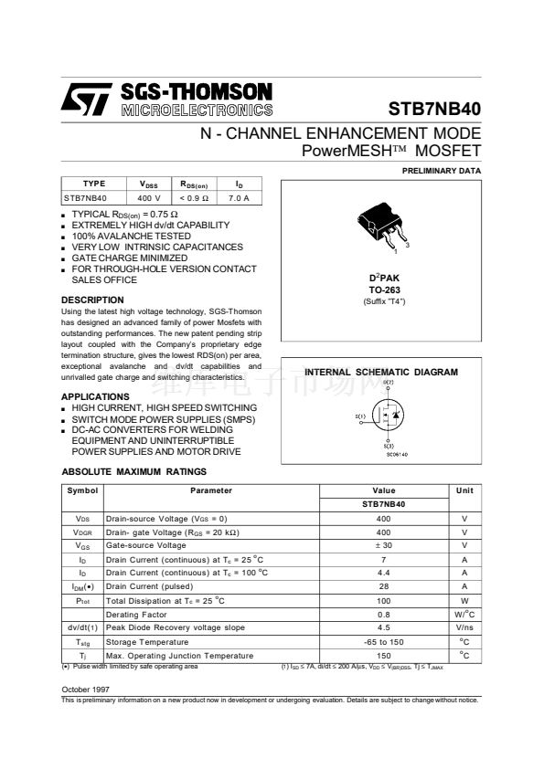
D
2
PAK
TO-263
(Suffix 鈥漈4鈥?
DESCRIPTION
Using the latest high voltage technology, SGS-Thomson
has designed an advanced family of power Mosfets with
outstanding performances. The new patent pending strip
layout coupled with the Company鈥檚 proprietary edge
termination structure, gives the lowest RDS(on) per area,
exceptional avalanche and dv/dt capabilities and
unrivalled gate charge and switching characteristics.
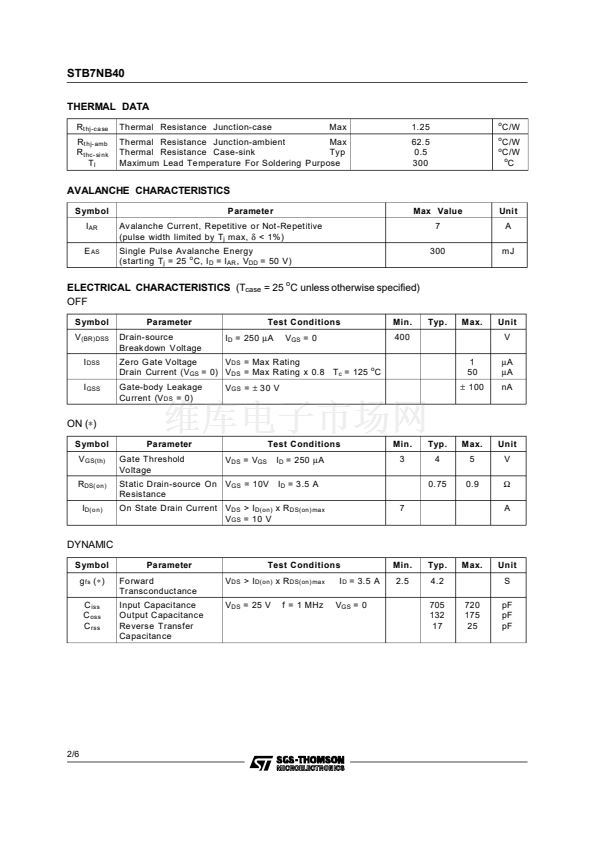
INTERNAL SCHEMATIC DIAGRAM
APPLICATIONS
s
HIGH CURRENT, HIGH SPEED SWITCHING
s
SWITCH MODE POWER SUPPLIES (SMPS)
s
DC-AC CONVERTERS FOR WELDING
EQUIPMENT AND UNINTERRUPTIBLE
POWER SUPPLIES AND MOTOR DRIVE
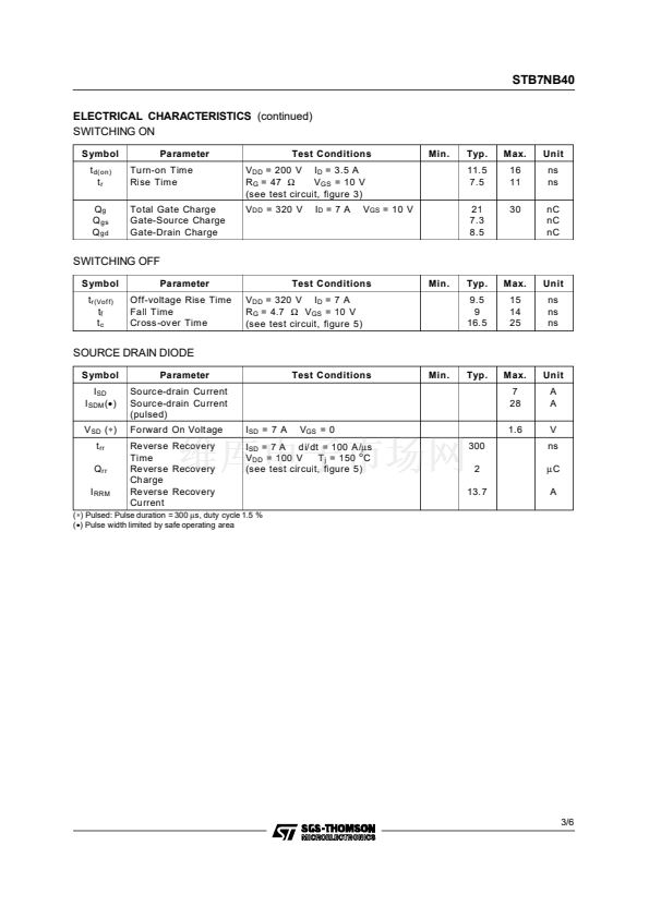
ABSOLUTE MAXIMUM RATINGS
Symbol
Parameter
Value
STB7NB40
V
DS
V
DGR
V
GS
I
D
I
D
I
DM
(鈥?
P
t ot
Drain-source Voltage (V
GS
= 0)
Drain- gate Voltage (R
GS
= 20 k鈩?
Gate-source Voltage
Drain Current (continuous) at T
c
= 25 C
Drain Current (continuous) at T
c
= 100
o
C
Drain Current (pulsed)
Total Dissipation at T
c
= 25 C
Derating F actor
dv/dt(
1
)
T
stg
T
j
Peak Diode Recovery voltage slope
Storage T emperature
Max. O perating Junction Temperature
o
o
Uni t
400
400
鹵
30
7
4.4
28
100
0.8
4.5
-65 to 150
150
(
1
) I
SD
鈮?/div>
7A, di/dt
鈮?/div>
200 A/碌s, V
DD
鈮?/div>
V
(BR)DSS
, Tj
鈮?/div>
T
JMAX
V
V
V
A
A
A
W
W/ C
V/ ns
o
o
o
C
C
(鈥? Pulse width limited by safe operating area
October 1997
This is preliminary information on a new product now in development or undergoing evaluation. Details are subject to change without notice.


 1
1
 2
2
 3
3
 4
4
 5
5
 6
6
