鈩?/div>
process, STMicroelectronis has designed an
advanced family of power MOSFETs with
outstanding performances. The new patent
pending strip layout coupled with the Company鈥檚
proprietary edge termination structure, gives the
lowest RDS(on) per area, exceptional avalanche
and dv/dt capabilities and unrivalled gate charge
and switching characteristics.
APPLICATIONS
s
HIGH CURRENT, HIGH SPEED SWITCHING
s
SWITCH MODE POWER SUPPLIES (SMPS)
s
DC-AC CONVERTERS FOR WELDING
EQUIPMENT AND UNINTERRUPTIBLE
POWER SUPPLIES AND MOTOR DRIVE
ABSOLUTE MAXIMUM RATINGS
Symb ol
V
DS
V
DGR
V
GS
I
D
I
D
I
DM
(鈥?
P
tot
dv/dt(
1
)
T
s tg
T
j
Parameter
Drain-source Voltage (V
GS
= 0)
Drain- gate Voltage (R
GS
= 20 k鈩?
G ate-source Voltage
Drain Current (continuous) at T
c
= 25
o
C
Drain Current (continuous) at T
c
= 100
o
C
Drain Current (pulsed)
T otal Dissipation at T
c
= 25 C
Derating Factor
Peak Diode Recovery voltage slope
Storage T emperature
Max. O perating Junct ion T emperature
o
D
2
PAK
TO-263
(suffix 鈥漈4鈥?
INTERNAL SCHEMATIC DIAGRAM
Value
200
200
鹵
30
10
6
40
85
0.68
5.5
-65 to 150
150
(
1
) I
SD
鈮?/div>
10A, di/dt
鈮?/div>
300 A/碌s, V
DD
鈮?/div>
V
(BR)DSS
, Tj
鈮?/div>
T
JMAX
Unit
V
V
V
A
A
A
W
W /
o
C
V/ns
o
o
C
C
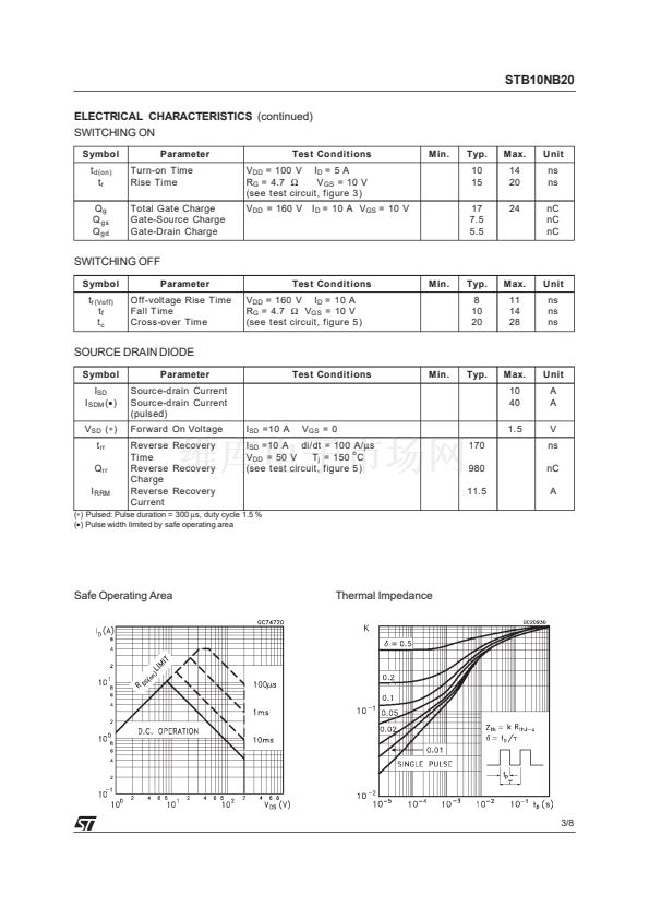
(鈥? Pulse width limited by safe operating area
November 1998
1/8


 1
1
 2
2
 3
3
 4
4
 5
5
 6
6
 7
7
 8
8
