廬
ST75C185
LOW POWER
MULTIPLE RS-232 DRIVERS AND RECEIVERS
TARGET DATA
s
s
s
s
s
s
s
s
s
s
MEETS STANDARD EIA-232-E
SINGLE CHIP WITH INTERFACE BETWEEN
UART AND SERIAL PORT CONNECTOR
LESS THAN 20mW QUIESCENT POWER
CONSUMPTION
WIDE DRIVER SUPPLY VOLTAGE: 7 TO 13.2V
DRIVER OUTPUT SLEW RATE LIMITED TO
30V/碌s MAX
RECEIVER INPUT HYSTERESIS: 1.1 TYP
PUSH-PULL RECEIVER OUTPUTS
ON CHIP RECEIVER 1碌s NOISE FILTER
FUNCTIONALLY INTERCHANGEABLE WITH
STM ST75185
ESD PROTECTION:
鹵10KV
HUMAN BODY
MODEL
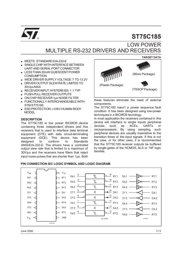
(Micro Package)
(Plastic Package)
(TSSOP Package)
DESCRIPTION
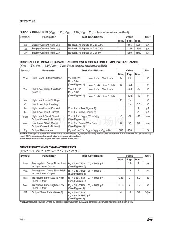
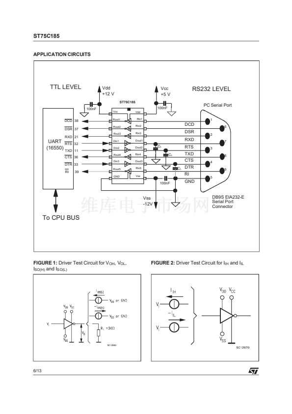
The ST75C185 is low power BICMOS device
containing three independent drivers and five
receivers that is used to interface data terminal
equipment (DTE) with data circuit-terminating
equipment (DCE). This device has been
designed
to
conform
to
Standards
ANSI/EIA-232-E. The drivers have a controlled
output slew rate that is limited to a maximum of
30V/碌s and the receivers have filters that reject
input noise pulses that are shorter than 1
碌
s. Both
these features eliminate the need of external
components.
The ST75C185 hasn鈥檛 a power sequence fault
condition. It has been designed using low-power
techniques in a BICMOS tecnology.
In most application the receivers contained in this
device will interface to single inputs peripheral
devices
such
as
ACEs,
UARTs
or
microprocessors. By using sampling, such
peripheral devices are usuallly insensitive to the
transition times of the input signals. If this is not
the case, or for other uses, it is recommended
that the ST75C185 receiver outputs be buffered
by single gates of the HCMOS, ALS or 74F logic
families.
PIN CONNECTION IEC LOGIC SYMBOL AND LOGIC DIAGRAM
June 2000
1/13


 1
1
 2
2
 3
3
 4
4
 5
5
 6
6
 7
7
 8
8
 9
9
 10
10
 11
11
 12
12
 13
13
