SSTUA32864
1.8 V con鏗乬urable registered buffer for DDR2-667 RDIMM
applications
Rev. 01 鈥?12 May 2005
Product data sheet
1. General description
The SSTUA32864 is a 25-bit 1 : 1 or 14-bit 1 : 2 con鏗乬urable registered buffer designed
for 1.7 V to 2.0 V V
DD
operation.
All clock and data inputs are compatible with the JEDEC standard for SSTL_18. The
control inputs are LVCMOS. All outputs are 1.8 V CMOS drivers that have been optimized
to drive the DDR2 DIMM load.
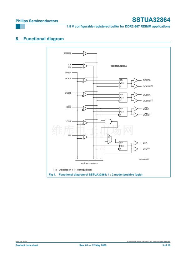
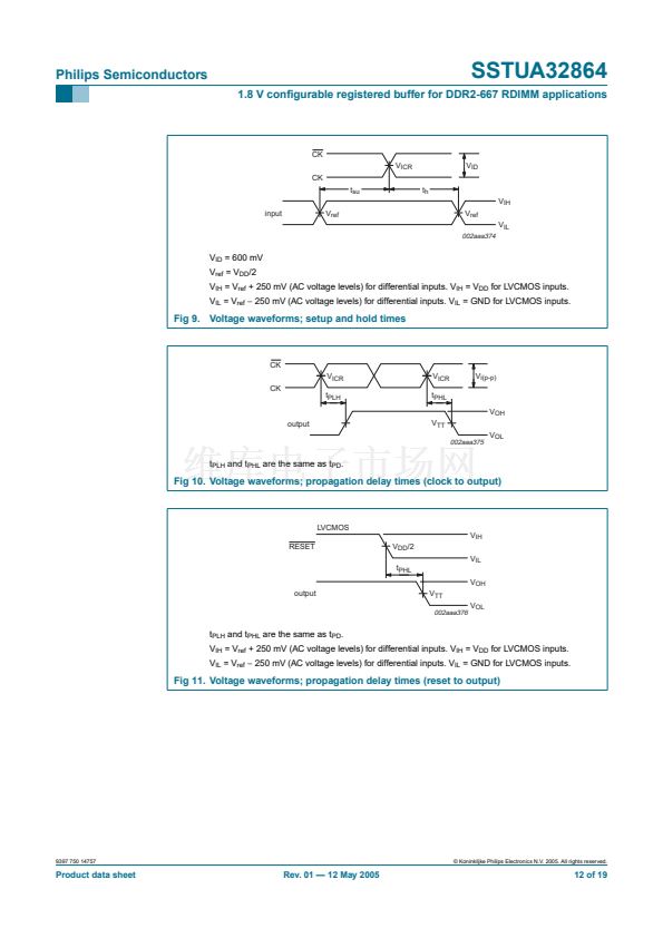
The SSTUA32864 operates from a differential clock (CK and CK). Data are registered at
the crossing of CK going HIGH, and CK going LOW.
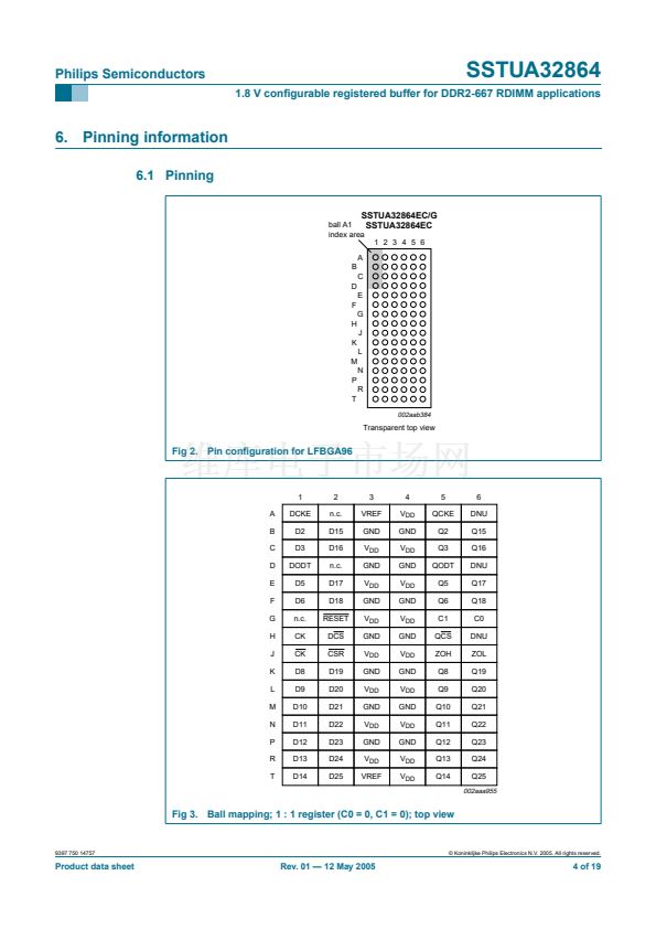
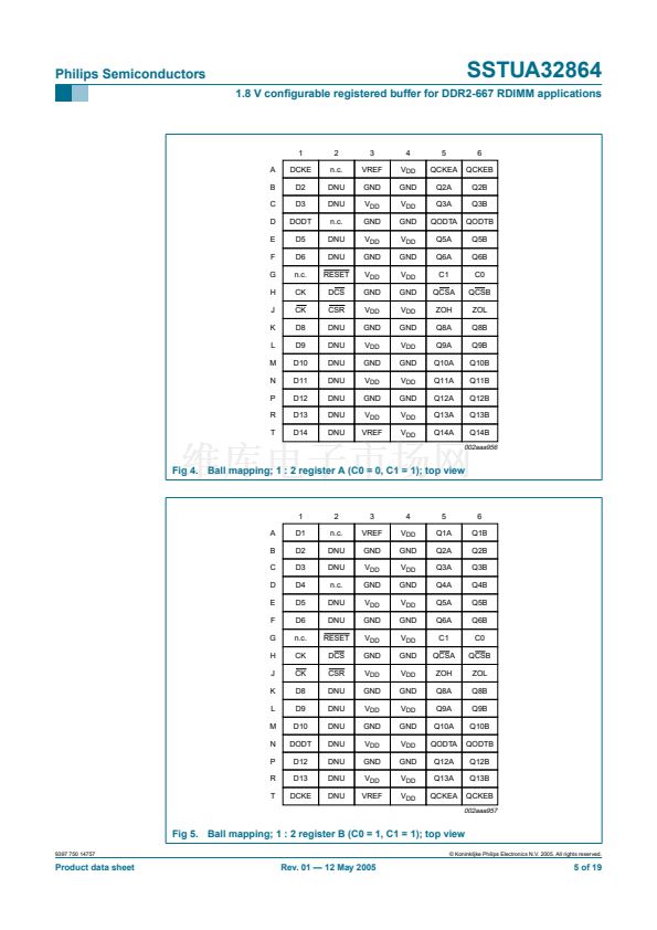
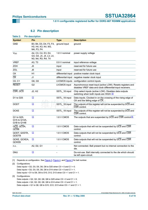
The C0 input controls the pinout con鏗乬uration of the 1 : 2 pinout from A con鏗乬uration
(when LOW) to B con鏗乬uration (when HIGH). The C1 input controls the pinout
con鏗乬uration from 25-bit 1 : 1 (when LOW) to 14-bit 1 : 2 (when HIGH).
The device supports low-power standby operation. When the reset input (RESET) is LOW,
the differential input receivers are disabled, and un-driven (鏗俹ating) data, clock and
reference voltage (VREF) inputs are allowed. In addition, when RESET is LOW all
registers are reset, and all outputs are forced LOW. The LVCMOS RESET and Cn inputs
must always be held at a valid logic HIGH or LOW level.
To ensure de鏗乶ed outputs from the register before a stable clock has been supplied,
RESET must be held in the LOW state during power-up.
In the DDR2 RDIMM application, RESET is speci鏗乪d to be completely asynchronous with
respect to CK and CK. Therefore, no timing relationship can be guaranteed between the
two. When entering reset, the register will be cleared and the data outputs will be driven
LOW quickly, relative to the time to disable the differential input receivers. However, when
coming out of reset, the register will become active quickly, relative to the time to enable
the differential input receivers. As long as the data inputs are LOW, and the clock is stable
during the time from the LOW-to-HIGH transition of RESET until the input receivers are
fully enabled, the design of the SSTUA32864 must ensure that the outputs will remain
LOW, thus ensuring no glitches on the output.
The device monitors both DCS and CSR inputs and will gate the Qn outputs from
changing states when both DCS and CSR inputs are HIGH. If either DCS or CSR input is
LOW, the Qn outputs will function normally. The RESET input has priority over the DCS
and CSR control and will force the outputs LOW. If the DCS-control functionality is not
desired, then the CSR input can be hardwired to ground, in which case the setup time
requirement for DCS would be the same as for the other Dn data inputs.
The SSTUA32864 is available in a 96-ball, low pro鏗乴e 鏗乶e-pitch ball grid array (LFBGA96)
package.


 1
1
 2
2
 3
3
 4
4
 5
5
 6
6
 7
7
 8
8
 9
9
 10
10
 11
11
 12
12
 13
13
 14
14
 15
15
 16
16
 17
17
 18
18
 19
19
