SSM6E01TU
TOSHIBA Multi-Chip Device
Silicon P-Channel MOS Type (U-MOS II) + N-Channel MOS Type (Planer)
SSM6E01TU
Load Switch Applications
路
路
P-channel MOSFET and N-channel MOSFET incorporated into one
package.
Low power dissipation due to P-channel MOSFET that features low
R
DS (ON)
and low-voltage operation
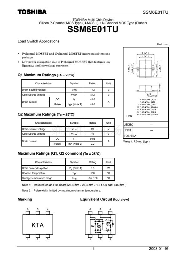
Unit: mm
Q1 Maximum Ratings
(Ta
=
25擄C)
Characteristics
Drain-Source voltage
Gate-Source voltage
Drain current
DC
Pulse
Symbol
V
DS
V
GSS
I
D
I
DP
(Note 2)
Rating
-12
鹵12
-1.0
-2.0
Unit
V
V
A
Q2 Maximum Ratings
(Ta
=
25擄C)
Characteristics
Drain-Source voltage
Gate-Source voltage
Drain current
DC
Pulse
Symbol
V
DS
V
GSS
I
D
I
DP
(Note 2)
Rating
20
10
0.05
0.2
Unit
V
V
A
JEDEC
JEITA
TOSHIBA
Weight: 7.0 mg (typ.)
鈥?/div>
鈥?/div>
鈥?/div>
Maximum Ratings (Q1, Q2 common)
(Ta
=
25擄C)
Characteristics
Drain power dissipation
Channel temperature
Storage temperature range
Symbol
P
D
(Note 1)
T
ch
T
stg
Rating
0.5
150
-55~150
Unit
W
擄C
擄C
2
Note 1: Mounted on an FR4 board (25.4 mm
麓
25.4 mm
麓
1.6 t, Cu pad: 645 mm )
Note 2: Pulse width limited by maximum channel temperature.
Marking
6
5
4
Equivalent Circuit
(top view)
6
5
4
Q1
KTA
1
2
3
1
Q2
2
3
1
2003-01-16


 1
1
 2
2
 3
3
 4
4
 5
5
 6
6
 7
7
 8
8
 9
9
