鈥?/div>
1.8 V drive
Low ON-resistance:
Unit: mm
R
on
= 134 m鈩?(max) (@V
GS
= 1.8V)
R
on
= 90 m鈩?(max) (@V
GS
= 2.5V)
R
on
= 74 m鈩?(max) (@V
GS
= 4.0V)
2.0鹵0.1
2.1鹵0.1
1.7鹵0.1
0.65鹵0.05
+0.1
0.3 -0.05
3
0.166鹵0.05
Absolute Maximum Ratings
(Ta = 25擄C)
Characteristic
Drain鈥搒ource voltage
Gate鈥搒ource voltage
Drain current
Drain power dissipation
Channel temperature
Storage temperature range
DC
Pulse
Symbol
V
DS
V
GSS
I
D
I
DP
P
D (Note 1)
P
D (Note 2)
T
ch
T
stg
Rating
30
鹵
12
2.5
5.0
800
500
150
鈭?5~150
Unit
V
V
1
2
mW
擄C
擄C
0.7鹵0.05
A
Using continuously under heavy loads (e.g. the application of
high temperature/current/voltage and the significant change in
temperature, etc.) may cause this product to decrease in the
reliability significantly even if the operating conditions (i.e.
operating temperature/current/voltage, etc.) are within the
absolute maximum ratings.
Please design the appropriate reliability upon reviewing the
Toshiba Semiconductor Reliability Handbook (鈥淗andling
Precautions鈥?鈥淒erating Concept and Methods鈥? and individual
reliability data (i.e. reliability test report and estimated failure
rate, etc).
Note 1: Mounted on a ceramic board.
2
(25.4 mm
脳
25.4 mm
脳
0.8 t, Cu Pad: 645 mm )
Note 2: Mounted on an FR4 board.
2
(25.4 mm
脳
25.4 mm
脳
1.6 t, Cu Pad: 645 mm )
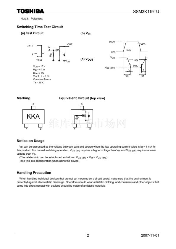
Note:
1: Gate
2: Source
3: Drain
UFM
JEDEC
JEITA
TOSHIBA
鈥?/div>
鈥?/div>
2-2U1A
Weight: 6.6 mg (typ.)
Electrical Characteristics
(Ta = 25擄C)
Characteristic
Drain鈥搒ource breakdown voltage
Drain cutoff current
Gate leakage current
Gate threshold voltage
Forward transfer admittance
Symbol
V
(BR) DSS
V
(BR) DSX
I
DSS
I
GSS
V
th
鈴怸
fs
鈴?/div>
R
DS (ON)
C
iss
C
oss
C
rss
t
on
t
off
V
DSF
Test Condition
I
D
=
1 mA, V
GS
=
0
I
D
=
1 mA, V
GS
=
鈥?2 V
V
DS
=
30 V, V
GS
=
0
V
GS
= 鹵
12 V, V
DS
=
0
V
DS
=
3 V, I
D
=
1 mA
V
DS
=
3 V, I
D
=
2 A
I
D
=
2.0 A, V
GS
=
4.0 V
Drain鈥搒ource ON-resistance
I
D
=
1.0 A, V
GS
=
2.5 V
I
D
=
0.5 A, V
GS
=
1.8 V
Input capacitance
Output capacitance
Reverse transfer capacitance
Switching time
Turn-on time
Turn-off time
V
DS
=
10 V, V
GS
=
0, f
=
1 MHz
V
DS
=
10 V, V
GS
=
0, f
=
1 MHz
V
DS
=
10 V, V
GS
=
0, f
=
1 MHz
V
DD
=
10 V, I
D
=
2 A,
V
GS
=
0 to 2.5 V, R
G
=
4.7
惟
I
D
= 鈭?/div>
2.5 A, V
GS
=
0 V
(Note3)
(Note3)
(Note3)
(Note3)
(Note3)
Min
30
18
鈳?/div>
鈳?/div>
0.4
3.8
鈳?/div>
鈳?/div>
鈳?/div>
鈳?/div>
鈳?/div>
鈳?/div>
鈳?/div>
鈳?/div>
鈳?/div>
Typ.
鈳?/div>
鈳?/div>
鈳?/div>
鈳?/div>
鈳?/div>
7.7
55
67
84
270
56
47
20
31
鈥?0.85
Max
鈳?/div>
鈳?/div>
1
鹵1
1.0
鈳?/div>
74
90
134
鈳?/div>
鈳?/div>
鈳?/div>
鈳?/div>
鈳?/div>
鈥?1.2
pF
pF
pF
ns
V
m惟
Unit
V
V
渭A
渭A
V
S
Drain鈥搒ource forward voltage
1
2007-11-01
SSM3K119TU相關(guān)型號(hào)PDF文件下載
-
型號(hào)
版本
描述
廠商
下載
-
英文版
High Speed Switching Applications
TOSHIBA
-
英文版
High Speed Switching Applications
TOSHIBA [T...
-
英文版
TOSHIBA Field Effect Transistor Silicon P Channel MOS Type
TOSHIBA
-
英文版
TOSHIBA Field Effect Transistor Silicon P Channel MOS Type
TOSHIBA [T...
-
英文版
TOSHIBA Field Effect Transistor Silicon P Channel MOS Type
TOSHIBA
-
英文版
TOSHIBA Field Effect Transistor Silicon P Channel MOS Type
TOSHIBA [T...
-
英文版
TOSHIBA Field Effect Transistor Silicon P Channel MOS Type
TOSHIBA
-
英文版
TOSHIBA Field Effect Transistor Silicon P Channel MOS Type
TOSHIBA [T...
-
英文版
TOSHIBA Field Effect Transistor Silicon P Channel MOS Type (...
TOSHIBA
-
英文版
TOSHIBA Field Effect Transistor Silicon P Channel MOS Type (...
TOSHIBA [T...
-
英文版
TOSHIBA Field Effect Transistor Silicon P Channel MOS Type (...
TOSHIBA
-
英文版
TOSHIBA Field Effect Transistor Silicon P Channel MOS Type (...
TOSHIBA [T...
-
英文版
TRANSISTOR | MOSFET | N-CHANNEL | 30V V(BR)DSS | 1.3A I(D) |...
ETC
-
英文版
HIGH SPEED SWITCHING APPLICATIONS
Toshiba
-
英文版
TOSHIBA Field Effect Transistor Silicon N Channel MOS Type
TOSHIBA
-
英文版
TOSHIBA Field Effect Transistor Silicon N Channel MOS Type
TOSHIBA [T...
-
英文版
TOSHIBA Field Effect Transistor Silicon N Channel MOS Type
TOSHIBA
-
英文版
TOSHIBA Field Effect Transistor Silicon N Channel MOS Type
TOSHIBA [T...
-
英文版
High Speed Switching Applications
TOSHIBA
-
英文版
Toshiba


 1
1
 2
2
 3
3
 4
4
 5
5
