鈥?/div>
Low power loss, high efficiency
Low profile surface mount package
Built-in strain relief
For use in low voltage high frequency inverters,
free wheeling, and polarity protection applications
鈥?Guardring for overvoltage protection
鈥?Plastic package has Underwriters Laboratory
Flammability Classification 94V-0
Parameter
Device marking code
Maximum repetitive peak reverse voltage
Maximum RMS voltage
Maximum DC blocking voltage
Maximum average forward rectified current at T
L
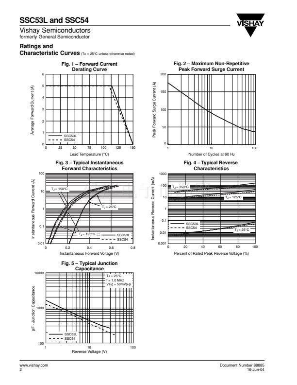
(See Fig. 1)
Mechanical Data
Case:
JEDEC DO-214AB molded plastic body
Terminals:
Solder plated, solderable per
MIL-STD750, Method 2026
High temperature soldering guaranteed:
250擄C/10 seconds at terminals
Polarity:
Color band denotes cathode end
Weight:
0.007 oz., 0.25 g
A
Maximum Ratings and Thermal Characteristics
(T
Symbol
V
RRM
V
RMS
V
DC
I
F(AV)
I
FSM
R
螛JA
R
螛JL
dv/dt
T
J
T
STG
(T
A
= 25擄C unless otherwise noted)
= 25擄C unless otherwise noted)
SSC53L
53L
30
21
30
5.0
175
60
20
10,000
鈥?5 to +150
鈥?5 to +150
SSC54
S54
40
28
40
Unit
V
V
V
A
A
擄C/W
V/碌s
擄C
擄C
Peak forward surge current 8.3ms single half sine-
wave superimposed on rated load (JEDEC Method)
Typical thermal resistance
(2)
Voltage rate of change (rated V
R
)
Operating junction temperature range
Storage temperature range
Electrical Characteristics
Parameter
Maximum instantaneous
Forward voltage at 5.0A
(1)
Maximum DC reverse current
at rated DC blocking voltage
(1)
Symbol
T
J
=25擄C
T
J
=125擄C
T
J
=25擄C
T
J
=125擄C
V
F
I
R
Typ.
0.42
0.33
鈥?/div>
45
Max.
0.45
0.38
0.7
65
Typ.
0.45
0.36
鈥?/div>
40
Max.
0.49
0.42
0.5
60
Unit
V
mA
Notes:
(1) Pulse test: 300碌s pulse width, 1% duty cycle
(2) Aluminum substrate mounted
Document Number 88885
16-Jun-04
www.vishay.com
1


 1
1
 2
2
