SS115
1.0 AMP. Surface Mount Schottky Barrier Rectifiers
Voltage Range
150 Volts
Current
1.0 Ampere
Features
a
a
a
a
a
a
a
a
For surface mounted application
Metal to silicon rectifier, majority carrier conduction
Low forward voltage drop
Easy pick and place
High surge current capability
Plastic material used carriers Underwriters
Laboratory Classification 94V-O
Epitaxial construction
High temperature soldering:
o
260 C/ 10 seconds at terminals
SMA/DO-214AC
.062(1.58)
.050(1.27)
.111(2.83)
.090(2.29)
.187(4.75)
.160(4.06)
Mechanical Data
a
a
a
a
a
Case: Molded plastic
Terminals: Solder plated
Polarity: Indicated by cathode band
Packaging: 12mm tape per EIA STD RS-481
Weight: 0.064 gram
.091(2.30)
.078(1.99)
.012(.31)
.006(.15)
.008(.20)
.004(.10)
.210(5.33)
.195(4.95)
.056(1.41)
.035(0.90)
Dimensions in inches and (millimeters)
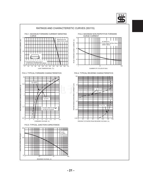
Maximum Ratings and Electrical Characteristics
Rating at 25+ambient temperature unless otherwise specified.
Single phase, half wave, 60 Hz, resistive or inductive load.
For capacitive load, derate current by 20%
Symbol
Type Number
Maximum Recurrent Peak Reverse Voltage
Maximum RMS Voltage
Maximum DC Blocking Voltage
Maximum Average Forward Rectified Current
at T
L
(See Fig. 1)
Peak Forward Surge Current, 8.3 ms Single Half
Sine-wave Superimposed on Rated Load
(JEDEC method )
Maximum Instantaneous Forward Voltage
O
(Note 1)
@ 25 C
1.0A
O
@ 125 C 1.0A
O
@ 25 C 2.0A
O
@ 125 C 2.0A
Maximum DC Reverse Current
@ T
A
=25+
at
SS115
150
105
150
1.0
30
0.82
0.67
0.89
0.75
0.05
0.5
50
20
-65 to +150
-65 to +150
Units
V
V
V
A
A
V
RRM
V
RMS
V
DC
I
(AV)
I
FSM
V
F
V
mA
mA
pF
+/W
+
+
Rated DC Blocking Voltage
@ T
A
=125+
Typical Junction Capacitance (Note 3)
Typical Thermal Resistance ( Note 2 )
Operating Temperature Range
Storage Temperature Range
I
R
Cj
R
JL
T
J
T
STG
Notes
:
1. Pulse Test with PW=300 usec, 1% Duty Cycle
2. Measured on P.C.Board with 0.2 x 0.2鈥?5.0 x 5.0mm) Copper Pad Areas.
3. Measured at 1 MHz and Applied Reverse Voltage of 4.0V D.C
- 908 -


 1
1
 2
2
