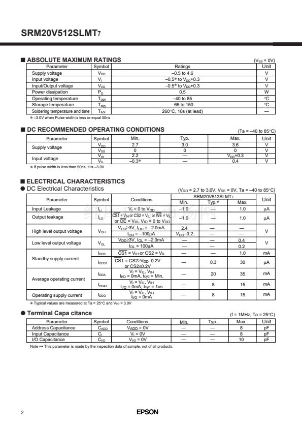
PF861-02
SRM20V512SLMT
7
512K-Bit Static RAM
ge
lta
Vo n
w ratio s
Lo pe ct
O odu
Pr
q
Wide Temperature Range
q
Low Supply Current
q
Access Time 70ns
q
65,536 words脳8 bit Asynchronous
s
DESCRIPTION
The SRM20V512SLMT
7
is a 65,536 words脳8-bit asynchronous, static, random access memory on a monolithic
CMOS chip. Its very low standby power requirement makes it ideal for applications requiring non-volatile storage
with back-up batteries. And 鈥?0 to 85擄C operating tempereture range wakes it idial for portable equipment. The
asynchronous and static nature of the memory requires no external clock or refreshing circuit. Both the input
and output ports are TTL compatible and the 3-state output allows easy expansion of memory capacity.
s
PIN CONFIGURATION
s
FEATURES
q
Wide tempereture range ................. 鈥?0 to 85擄C
q
Fast Access time ............................. SRM20V512SLMT
7
70ns
q
Low supply current .......................... standby : 0.3碌A(chǔ) (Typ.)
operation : 8mA/1MHz (Typ.)
q
Completely static ............................. No clock required
q
Single power supply ........................ 2.7V to 3.6V
q
TTL compatible inputs and outputs
q
3-state output with wired-OR capability
q
Non-volatile storage with back-up batteries
q
Package ...... SRM20V512SLMT
7
SOP6-32pin (plastic)
SRM20V512SLTT
7
TSOP (
I
)-32pin (plastic)
SRM20V512SLRT
7
TSOP (
I
)-32pin-R1 (plastic)
SRM20V512SLKT
7
Slim-TSOP (
I
)-32pin (plastic)
SRM20V512SLYT
7
Slim-TSOP (
I
)-32pin-R1 (plastic)
(SOP6)
N.C.
N.C.
A14
A12
A7
A6
A5
A4
A3
A2
A1
A0
I/01
I/02
I/03
V
SS
1
2
3
4
5
6
7
8
9
10
11
12
13
14
15
16
32
31
30
29
28
27
26
25
24
23
22
21
20
19
18
17
V
DD
A15
CS2
WE
A13
A8
A9
A11
OE
A10
CS1
I/08
I/07
I/06
I/05
I/04
SRM20V512SLMT
(TSOP/Slim-TSOP)
A11
A9
A8
A13
WE
CS2
A15
V
DD
N.C.
N.C.
A14
A12
A7
A6
A5
A4
1
2
3
4
5
6
7
8
9
10
11
12
13
14
15
16
32
31
30
29
28
27
26
25
24
23
22
21
20
19
18
17
OE
A10
CS1
I/08
I/07
I/06
I/05
I/04
V
SS
I/03
I/02
I/01
A0
A1
A2
A3
SRM20V512SLTT/KT
s
BLOCK DIAGRAM
A0
A1
A2
A3
A4
A5
A6
A7
A8
A9
A10
A11
A12
A13
A14
A15
CS1
CS2
(TSOP-R1/Slim-TSOP-R1)
A4
A5
A6
A7
A12
A14
N.C.
N.C.
V
DD
A15
CS2
WE
A13
A8
A9
A11
16
15
14
13
12
11
10
9
8
7
6
5
4
3
2
1
17
18
19
20
21
22
23
24
25
26
27
28
29
30
31
32
A3
A2
A1
A0
I/01
I/02
I/03
V
SS
I/04
I/05
I/06
I/07
I/08
CS1
A10
OE
X Decoder
9
512
Memory Cell Array
512脳128脳8
Address Buffer
SRM20V512SLRT/YT
128脳8
7
Y
Decoder
128
Column Gate
s
PIN DESCRIPTION
CS1, CS2
Control
Logic
8
OE
WE
I/O Buffer
I/O1 I/O2 I/O3 I/O4 I/O5 I/O6 I/O7 I/O8
A0 to A15
WE
OE
CS1
CS2
I/O1 to 8
V
DD
V
SS
N. C.
Address Input
Write Enable
Output Enable
Chip Select 1
Chip Select 2
Data I/O
Power Supply (2.7V to 3.6V)
Power Supply (0V)
No connection
OE, WE
Control
Logic


 1
1
 2
2
 3
3
 4
4
 5
5
 6
6
 7
7
 8
8
