鈥?/div>
Compact type : H3.25
!
L5.0
!
W4.5mm
Absolute Maximum Ratings at Ta=25
擄
C, 65%RH
Parameter
Forward Current
Reverse Voltage
Power Dissipation
Collector-Emitter Voltage
Emitter-Collector Voltage
Collector Curren
Power Dissipation
Operating Temperature
Storage Temperature
Soldering Temperature
*1
Symbol
I
F
V
R
P
D
V
CEO
V
ECO
I
C
P
C
Topr
Tstg
Tsol
Rating
50
5
70
20
5
20
70
- to +80
-20
- to +85
-30
260
Unit
mA
V
mW
V
V
mA
mW
擄C
擄C
擄C
Input LED
Output
Phototransistor
*1
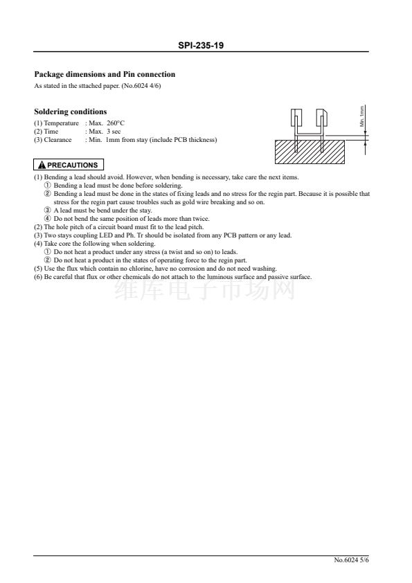
Soldering conditions : time : max. 3sec; clearance : min. 1mm from lower stay
Electro-Optical Characteristics at Ta=25
擄
C, 65%RH
Parameter
Forward Voltage
Reverse Current
Dark Current
Collector Output Current
Collector Emitter
Saturation Voltage
Symbol
V
F
I
R
I
CEO
I
C
V
CE
(sat)
Condition
I
F
=10mA
V
R
=5V
I
F
=0mA, V
CE
=10V
I
F
=10mA,V
CE
=5V
*1
I
F
=10mA, I
C
=100碌A(chǔ)
V
CC
=5V, R
L
=100鈩?/div>
I
C
=1mA
Min.
1.0
-
-
-
-
200
-
-
-
-
-
-
Typ.
1.15
-
-
10
-
-
-
-
7
7
VCE=5V
IF=10mA
Ic
A
Input
Output
Max.
1.4
10
200
1000
0.5
--
--
Unit
V
碌A(chǔ)
nA
碌A(chǔ)
V
碌s
碌s
Coupled
Rise Time
tr
Fall Time
tf
*1
Measurement Circuit of Collector Current
*2
Table
of Classification of Collector Output
Class
A
B
C
Ic (碌A(chǔ))
1000 to 450 650 to 300 450 to 200
SANYO Electric Co.,Ltd. Semiconductor Company
TOKYO OFFICE Tokyo Bldg., 1-10, 1 Chome, Ueno, Taito-ku, TOKYO, 110-8534 JAPAN
72199 GI, (MI) No.6024 1/6


 1
1
 2
2
 3
3
 4
4
 5
5
 6
6
