鈻?/div>
Serial interface protocol circuits
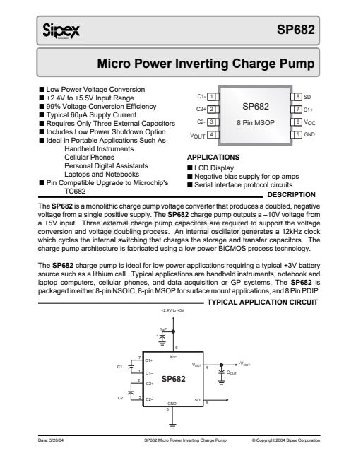
DESCRIPTION
The
SP682
is a monolithic charge pump voltage converter that produces a doubled, negative
voltage from a single positive supply. The
SP682
charge pump outputs a 鈥?0V voltage from
a +5V input. Three external charge pump capacitors are required to support the voltage
conversion and voltage doubling process. An internal oscillator generates a 12kHz clock
which cycles the internal switching that charges the storage and transfer capacitors. The
charge pump architecture is fabricated using a low power BiCMOS process technology.
The
SP682
charge pump is ideal for low power applications requiring a typical +3V battery
source such as a lithium cell. Typical applications are handheld instruments, notebook and
laptop computers, cellular phones, and data acquisition or GP systems. The
SP682
is
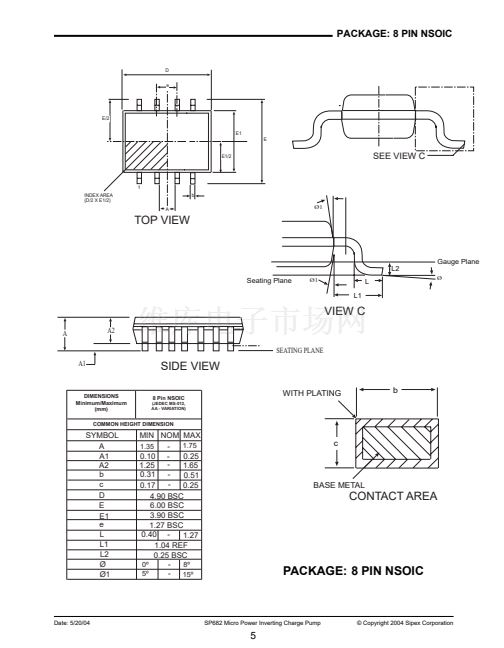
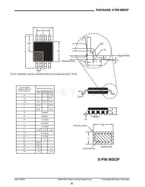
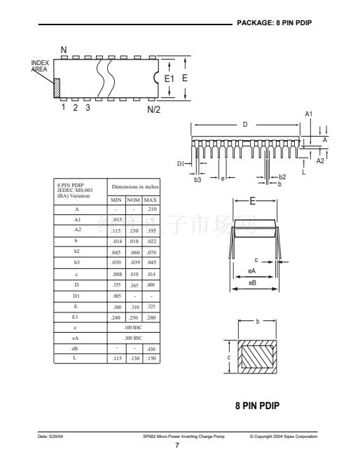
packaged in either 8-pin NSOIC, 8-pin MSOP for surface mount applications, and 8 Pin PDIP.
TYPICAL APPLICATION CIRCUIT
+2.4V to +5V
1碌F
+
6
7
C1
1
2
C1鈥?/div>
C2+
C1+
V
CC
V
OUT
4
-
V
OUT
C
OUT
SP682
SD
GND
5
8
C2
3
C2鈥?/div>
Date: 5/20/04
SP682 Micro Power Inverting Charge Pump
漏 Copyright 2004 Sipex Corporation
1


 1
1
 2
2
 3
3
 4
4
 5
5
 6
6
 7
7
 8
8
